

Display substrate, manufacture method thereof, display panel and mask plate
By introducing an auxiliary electrode in parallel with the cathode layer in the organic light-emitting diode display panel and optimizing the deposition position of the cathode layer, the problem of resistance voltage drop of the cathode layer is solved and the picture quality is improved.
- Summary
- Abstract
- Description
- Claims
- Application Information
AI Technical Summary
Problems solved by technology
Method used
Image

Examples
Embodiment approach
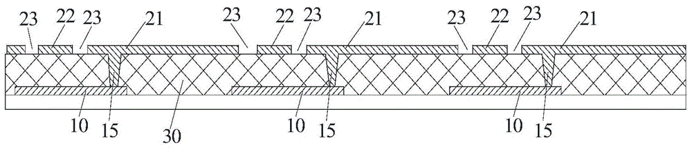
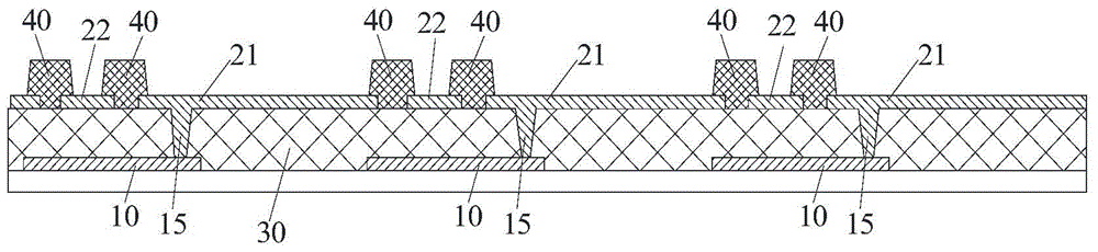
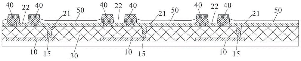
[0073] As a preferred embodiment of the present invention, the display substrate may further include a spacer 40 that insulates and separates the auxiliary electrode 22 from the anode 21 . The spacer 40 can ensure that the auxiliary electrode 22 is reliably insulated from the anode 21 . In the present invention, the specific shape of the spacer 40 is not specifically limited, as long as it can insulate and space the auxiliary electrode 22 from the anode 21 . Specifically, an insulating space 23 is respectively formed on both sides of each auxiliary electrode 22, and a spacer 40 is arranged in each of the insulating space 23, and a part of the spacer 40 is set in the corresponding insulating space 23, and the other part It protrudes from the anode layer to insulate the auxiliary electrode 22 from the adjacent anode 21 .
[0074] As mentioned above, the auxiliary electrode 22 should be arranged at a position that does not affect the normal light emission of the display panel. ...
PUM
 Abstract
Description
Claims
Application Information