Ultra wide band antenna with trapped wave features

A technology of ultra-wideband antenna and notch wave characteristics, which is applied in the directions of antenna coupling, antenna grounding device, radiating element structure, etc., and can solve the problem of mismatching between antenna and microwave circuit, endangering the normal operation of the system, complex antenna structure and process, etc. problems, to achieve low production costs, reduce design costs, and facilitate mass production

Inactive Publication Date: 2015-06-03
HARBIN HESON SCI & TECH
View PDF0 Cites 1 Cited by
  • Summary
  • Abstract
  • Description
  • Claims
  • Application Information

AI Technical Summary

Problems solved by technology

[0003] However, the frequency band occupied by the current ultra-wideband communication has a common part with the wireless local area network, so it is necessary to design an antenna that can reduce the interference to the wireless local area network. Designing an ultra-wideband antenna with notch characteristics has become a current research hotspot.
If there is no proper design to suppress harmonic resonance and spurious emission, the antenna will cause electromagnetic interference to nearby equipment, endangering the normal operation of the system itself and adjacent systems, especially causing interference to the currently used LAN system
Adding a filter is the most commonly used method to solve this kind of problem, but it often causes a mismatch between the antenna and the microwave circuit, and even reduces the overall performance of the system. Therefore, designing an ultra-wideband antenna with notch characteristics is the best way to solve this problem. One of the important methods, while solving the current complex problems of the structure and technology of the antenna

Method used


Image

  • Ultra wide band antenna with trapped wave features
  • Ultra wide band antenna with trapped wave features
  • Ultra wide band antenna with trapped wave features

Examples


Embodiment 1

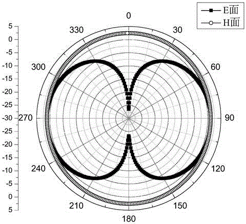
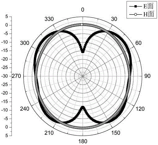
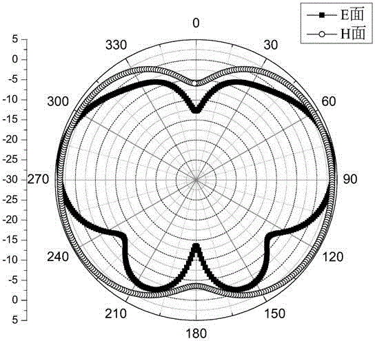
[0025] like figure 1 As shown, the UWB antenna with notch characteristics consists of: a dielectric substrate (1), a radiation element (2), a coplanar waveguide signal feeding stripline (3), and a coplanar waveguide ground plane (4) , open a U-shaped slot (5) on the signal feeder strip line. The radiating unit, the coplanar waveguide signal feeding stripline, and the coplanar waveguide ground plane are printed on the upper surface of the dielectric substrate; the radiating unit is located in the middle of the dielectric substrate, and the coplanar waveguide feeding stripline is led from the edge of the dielectric substrate. The ground plane of the coplanar waveguide is composed of two pieces of trapezoidal metal, which are respectively fixed on both sides of the coplanar waveguide feeding stripline and have a gap with the stripline.

[0026] The dielectric substrate is made of polytetrafluoroethylene with a thickness of 1.6 mm and a relative dielectric constant of 4.4.

[00...


PUM


Abstract

The invention discloses an ultra wide band antenna with trapped wave features. The ultra wide band antenna comprises a medium base plate (1), a radiation unit (2), a coplane waveguide signal feeding belt line (3) and a coplane waveguide grounding surface (4), wherein a U-shaped groove (5) is formed in the signal feeding belt line. The radiation unit, the coplane waveguide signal feeding belt line and the coplane waveguide grounding surface are printed on the upper surface of the medium base plate, the radiation unit is positioned in the middle part of the medium base plate, the coplane waveguide signal feeding belt line is led to the radiation unit from the medium base plate from the edge of the medium base plate and is connected with the radiation unit, the coplane waveguide grounding surface consists of two approximately trapezoidal metals, the two approximately trapezoidal metals are respectively and fixedly arranged at the two sides of the coplane waveguide signal feeding belt line, and gaps are formed between the metals and the belt line. The ultra wide band antenna has the advantages that the structure is compact, the dimension is small, the structure is ingenious, the trapped wave frequency can be regulated through changing the dimension and the position of the U-shaped groove, and the problem of same-frequency interference of an ultra wide band communication system is solved.

Description

technical field [0001] The invention designs an antenna, in particular to an ultra-wideband antenna with notch characteristics. Background technique [0002] Since the US Federal Communications Commission (Federal Communications Commission) allowed the commercial use of the 3.1-10.6GHz frequency band, ultra-wideband technology has received wider attention in the academic and commercial fields. The coplanar waveguide structure that does not require drilling and is easy to integrate is changing day by day, and the structure can be fabricated by photographic technology and has good polarization characteristics, so this technology has been applied to the design of ultra-wideband antennas and related microwave circuit components in the design. [0003] However, the frequency band occupied by the current ultra-wideband communication and the wireless local area network share a part, so it is necessary to design an antenna that can reduce the interference to the wireless local area...

Claims


Application Information

Patent Timeline
Patent Type & Authority Applications(China)
IPC IPC(8): H01Q1/38H01Q1/52H01Q1/48
Inventor 李琦金佳佳张冰然
Owner HARBIN HESON SCI & TECH
Why Eureka
Try Eureka