

Shift register, gate drive circuit unit, gate drive circuit and display
A gate drive circuit, shift register technology, applied in static memory, static indicator, digital memory information and other directions, can solve the problem of unfavorable display panels, large area occupied by gate drive circuits, and decreased yield of gate drive circuits and other problems, to achieve the effect of reducing the number, improving the circuit yield, and reducing the cost of the circuit
- Summary
- Abstract
- Description
- Claims
- Application Information
AI Technical Summary
Problems solved by technology
Method used
Image

Examples
Embodiment 1
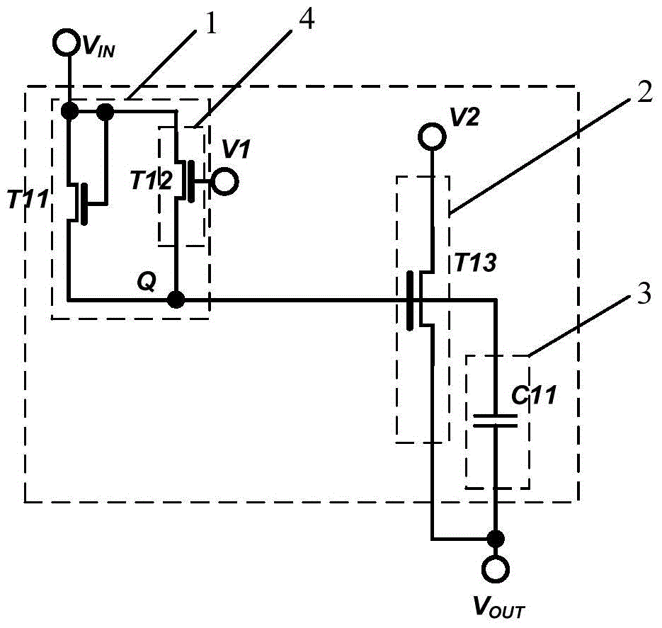
[0051] Please refer to figure 2 , the shift register in this embodiment includes a signal input module 1 , a signal output module 2 , a pull-up module 3 and a reset module 4 .
[0052] Signal input module 1 is used to receive the external start signal V IN and the first clock signal V1, and the signal output module 2 is turned on; the first input terminal of the signal output module 2 and the output terminal of the signal input module 1 are coupled to the first node Q, and the second input terminal of the signal output module 2 is used To receive the second external clock signal V2, the output terminal of the signal output module 2 is used to output the scan signal V after the module is turned on OUT ; One end of the pull-up module 3 is coupled to the first node Q, and the other end is coupled to the output end of the signal output module 2, the pull-up module 3 is used to increase the voltage of the first node Q; the reset module 4 is used to reset the first node Q The vol...
Embodiment 2
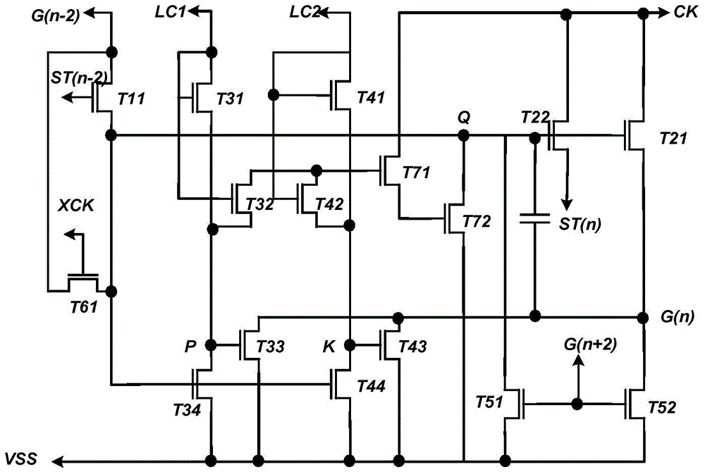
[0059] Please refer to image 3 , the gate drive circuit unit of this embodiment includes a pull-down module and a plurality of cascaded shift registers, the plurality of shift registers share the pull-down module, and the pull-down module is used to pull the scan signal output by the signal output module to a low level . The current-stage clock signals of multiple shift registers must have the same period and equal duty cycle, and there is an overlapping part in the time domain between the current-stage clock signals of adjacent shift registers. The more cascaded shift register stages, the fewer transistors are required on average for each stage of shift register. However, if there are too many cascaded stages in practical applications, the upper stage that should be in a low-level maintenance state will The voltage of the first node will be in a suspended state due to too many stages causing the voltage of the second node to remain at a high level, which may cause abnormal ...
Embodiment 3
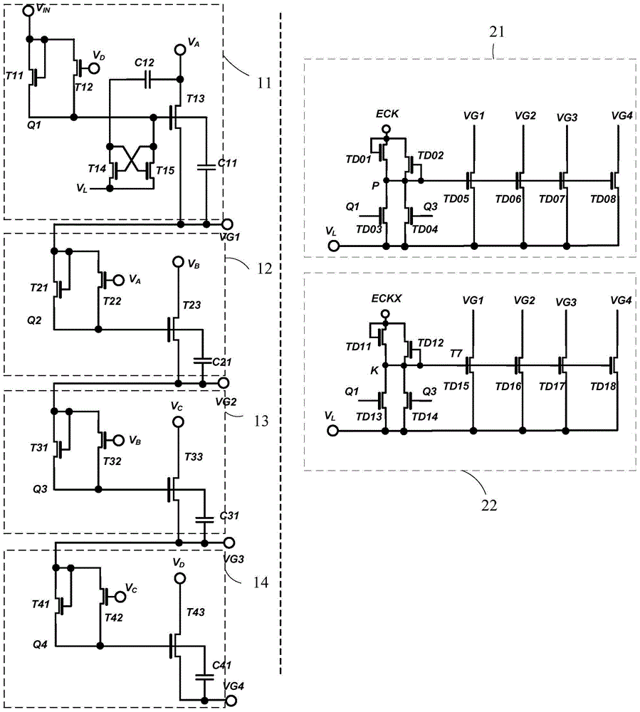
[0080] Please refer to Image 6 , the gate drive circuit unit in this embodiment includes 4 stages of cascaded shift registers (the first stage shift register 31, the second stage shift register 32, the third stage shift register 33 and the fourth stage shift register The register 34 ), the first pull-down circuit 41 , and the second pull-down circuit 42 are connected in the same way as in the second embodiment, and will not be repeated here. The difference between this embodiment and the second embodiment is that each stage of shift register does not include the first capacitor. Because in the low-level maintenance phase, the voltage jump amplitude on the first node is related to the voltage division between the first capacitor and the gate-drain parasitic capacitance of the third transistor, the existence of the first capacitor can further improve the clock feedthrough effect of the circuit. suppression. However, when the size of the third transistor is large (the width is...
PUM
 Abstract
Description
Claims
Application Information