Forming method of fin field-effect transistor

A fin field effect and transistor technology, which is applied in semiconductor devices, semiconductor/solid state device manufacturing, electrical components, etc., can solve the problems of source-drain punch-through, affecting the performance of fin field effect transistors, etc., to improve quality and improve diffusion barrier role, the effect of reducing the spread

Active Publication Date: 2015-06-10
SEMICON MFG INT (SHANGHAI) CORP
View PDF5 Cites 21 Cited by
  • Summary
  • Abstract
  • Description
  • Claims
  • Application Information

AI Technical Summary

Problems solved by technology

[0005] The phenomenon of source-drain punch-through often occurs between the source and the drain of the fin...

Method used


Image

  • Forming method of fin field-effect transistor
  • Forming method of fin field-effect transistor
  • Forming method of fin field-effect transistor

Examples


Embodiment Construction

[0032] As mentioned in the background art, the fin field effect transistor formed in the prior art is prone to source-drain punchthrough phenomenon, which affects the performance of the fin field effect transistor.

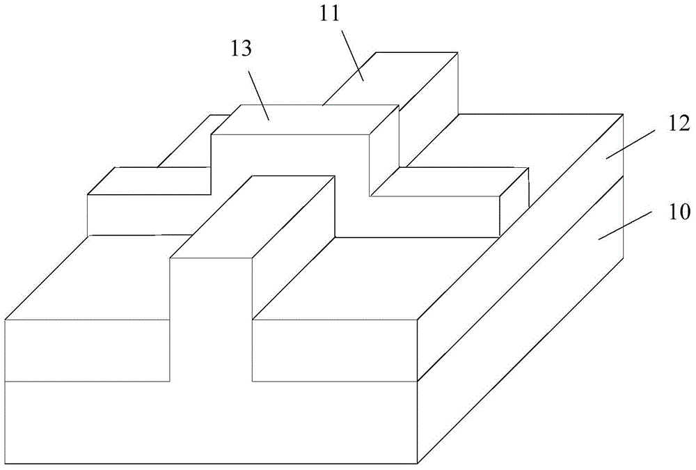
[0033] In an embodiment of forming a Fin Field Effect Transistor, after ion implantation is performed on the semiconductor substrate to form a punch-through barrier layer, the semiconductor substrate is etched to form a fin, so that the fin has a punch-through barrier layer, which can improve The punch-through voltage between source and drain.

[0034] However, studies have found that the dopant ions in the punch-through barrier layer will diffuse outward during the formation of the fin field effect transistor, and finally reduce the ion doping concentration in the punch-through barrier layer, so that the source-drain punch-through The blocking effect is reduced. This is mainly due to the fact that in the process steps after the formation of the fins, multiple he...


PUM


Abstract

A forming method of a fin field-effect transistor includes: providing a semiconductor substrate comprising an NMOS (N-channel metal oxide semiconductor) area and a PMOS (P-channel metal oxide semiconductor) area; etching the semiconductor substrate to form a first fin portion in the NMOS area and a second fin portion in the PMOS area; forming a dielectric layer on the surface of the first and second fin portions, with the surface of the dielectric layer being flush with the top of the first and second fin portions; subjecting the second fin portion to second ion implanting to form a second through barrier layer in the second fin portion; subjecting the first fin portion to first ion implanting to form a first through barrier layer in the first fin portion; removing part, of certain thickness, of the dielectric layer so that the surface of the dielectric layer is flush with the surface of the first and second through barrier layers or lower than the first and second through barrier layers. The forming method has the advantages that breakthrough between a source and a drain can be avoided and the performance of the fin field-effect transistor is improved.

Description

technical field [0001] The invention relates to the technical field of semiconductors, in particular to a method for forming a fin field effect transistor. Background technique [0002] With the continuous development of semiconductor process technology, the process node is gradually reduced, and the gate-last (gate-last) process has been widely used to obtain an ideal threshold voltage and improve device performance. However, when the feature size of the device is further reduced, even if the gate-last process is adopted, the structure of the conventional MOS field effect transistor can no longer meet the requirements for device performance. Fin field effect transistor (Fin FET) is obtained as a multi-gate device. received widespread attention. [0003] Fin field effect transistor is a common multi-gate device, figure 1 A schematic diagram of a three-dimensional structure of a fin field effect transistor in the prior art is shown. [0004] Such as figure 1 As shown, it ...

Claims


Application Information

Patent Timeline
IPC IPC(8): H01L21/336
CPCH01L29/66795H01L29/7854
Inventor 谢欣云洪中山
Owner SEMICON MFG INT (SHANGHAI) CORP
Why Eureka
Try Eureka