Supercharge Your Innovation With Domain-Expert AI Agents!

Display substrate, display panel and display device

一种显示基板、显示面板的技术,应用在测量装置、静态指示器、仪器等方向,能够解决降低显示面板生产效率、显示面板厚度增加、信号线信号异常等问题,达到防止腐蚀、降低厚度、提高生产效率的效果

Active Publication Date: 2015-06-24
BOE TECH GRP CO LTD +1
View PDF4 Cites 11 Cited by
  • Summary
  • Abstract
  • Description
  • Claims
  • Application Information

AI Technical Summary

Problems solved by technology

[0004] In the above-mentioned display substrate, the test point on the test pad 2 is an exposed conductive metal area, which is easily corroded in the atmosphere, and the corrosion of the test point will cause abnormal signals in the signal line, which will cause the display panel to be damaged. damage
Therefore, after the detection of the display panel is completed, it is necessary to apply UV glue at the test pad 2 to protect the circuit and avoid corrosion of the test points; obviously, coating the UV glue at the test pad 2 will reduce the production of the display panel Efficiency, reduce productivity, and also lead to increase in the thickness of the display panel

Method used


Image

  • Display substrate, display panel and display device
  • Display substrate, display panel and display device
  • Display substrate, display panel and display device

Examples


Embodiment Construction

[0027] Specific embodiments of the present invention will be described in detail below in conjunction with the accompanying drawings. It should be understood that the specific embodiments described here are only used to illustrate and explain the present invention, and are not intended to limit the present invention.

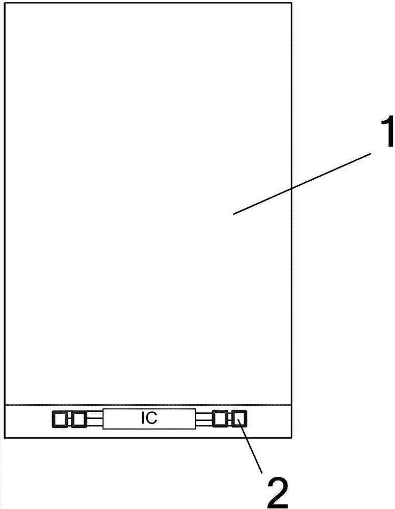
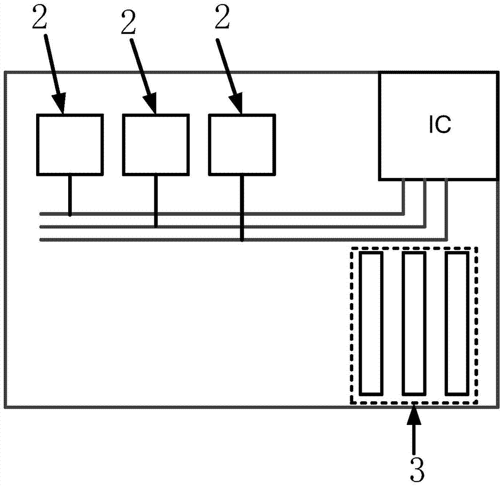
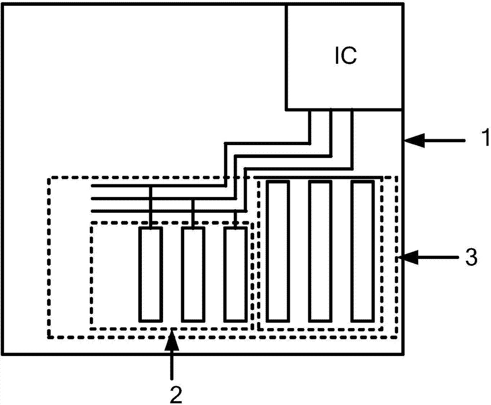
[0028] The present invention provides an embodiment of a display substrate, image 3 It is a schematic diagram of a display substrate provided by an embodiment of the present invention. Such as figure 1 As shown, in this embodiment, the display substrate 1 includes a flexible circuit board 3 and a test pad 2 , and the flexible circuit board 3 covers the area where the test pad 2 is located. Specifically, the display substrate 1 is generally an array substrate.

[0029] When preparing the display substrate, after the thin film transistors, pixel electrodes, and signal lines such as gate lines and data lines are prepared, the test probes are brought into contac...


PUM


Abstract

The invention relates to a display substrate, a display panel and a display device. The display substrate comprises a flexible circuit board and a test bonding pad, and the flexible circuit board covers an area of the test bonding pad, so that test points on the test bonding pad can be prevented from contacting with an external environment so as to be protected from corrosion, and signal abnormality, caused by corrosion of the test points, of signal lines in a display process can be avoided. Compared with the prior art, the display substrate has the advantages that a process of coating UV (ultraviolet) adhesive onto the test bonding pad is saved, technical procedures are reduced, production efficiency and productivity are improved, and thickness of the display substrate can be reduced to make the display panel thinner.

Description

technical field [0001] The present invention relates to the field of display technology, in particular to a display substrate, a display panel including the display substrate, and a display device including the display panel. Background technique [0002] After the display panel is prepared, the display panel needs to be inspected to determine whether there is a defect in the display panel. For the convenience of detection, a test pad (pad) is generally arranged on the display substrate (usually an array substrate). During detection, a test probe is used to contact the test point on the test pad, and the test point is connected to the signal line. connected, so that a detection signal can be input into the signal line through the test probe and the test point to detect whether there is a defect in the display panel. [0003] figure 1 is a schematic diagram of an existing display substrate; figure 2 for figure 1 A schematic showing the test pads in the substrate is shown...

Claims


Application Information

Patent Timeline
Patent Type & Authority Applications(China)
IPC IPC(8): G09G3/00
CPCG01R31/2818G01R31/2884G02F1/13458G09G3/006G09G2300/0426G09G2330/12H01L27/1218H01L27/124
Inventor 董学马磊薛海林朱海波李月姜文博杨东杨明
Owner BOE TECH GRP CO LTD
Features
  • R&D
  • Intellectual Property
  • Life Sciences
  • Materials
  • Tech Scout
  • Unparalleled Data Quality
  • Higher Quality Content
  • 60% Fewer Hallucinations
Learn More