Through silicon via forming method and alignment structure of semiconductor device

A semiconductor and through-silicon via technology, which is applied in semiconductor devices, semiconductor/solid-state device manufacturing, semiconductor/solid-state device components, etc., can solve problems such as metal diffusion, adverse effects on semiconductor device performance, and difficult alignment

Active Publication Date: 2015-06-24
SEMICON MFG INT (SHANGHAI) CORP
View PDF6 Cites 7 Cited by
  • Summary
  • Abstract
  • Description
  • Claims
  • Application Information

AI Technical Summary

Problems solved by technology

[0006] The above existing methods for forming TSVs have the following disadvantages: in the above alignment structure, the metal layer 13b, the nitride layer 16 and the insulating layer 17 have flush surfaces, so it is difficult to perform alignment quickly and accurately
[0007] In addition, the direct lamination between the existing metal interconnection layer 12 and the interlayer dielectric layer 11 is likely to cause the metal in

Method used


Image

  • Through silicon via forming method and alignment structure of semiconductor device
  • Through silicon via forming method and alignment structure of semiconductor device
  • Through silicon via forming method and alignment structure of semiconductor device

Examples


Embodiment Construction

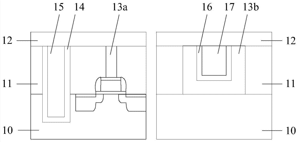
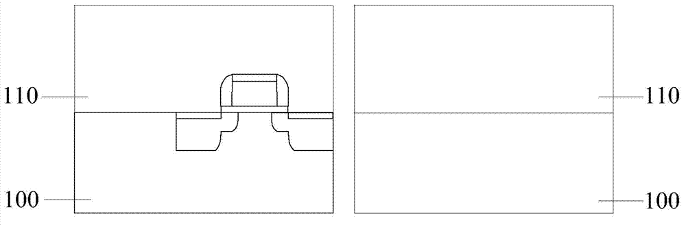
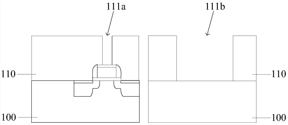
[0051]As mentioned in the background technology, in the existing through-silicon via formation method, the metal interconnection layer and the interlayer dielectric layer are directly stacked, which easily causes the metal in the metal interconnection layer to diffuse into the interlayer dielectric layer, which affects the performance of the semiconductor device. Cause adverse effects; it needs to be planarized to expose the surface of the interlayer dielectric layer to expose the conductive column, the interlayer dielectric layer is easy to be flatly removed during the planarization process and it is difficult to stop accurately; in the alignment structure, the metal layer, nitride layer and insulation The layers have flush surfaces, making quick and precise alignment difficult.

[0052] Therefore, the present invention provides a new method for forming TSVs. In the process of forming TSVs, a sacrificial layer is firstly formed to fill the grooves, thereby preventing the subse...


PUM

PropertyMeasurementUnit
Thicknessaaaaaaaaaa

Abstract

A through silicon via forming method and an alignment structure of a semiconductor device are provided. The semiconductor device comprises a semiconductor substrate and an interlayer dielectric layer disposed on the semiconductor substrate. The interlayer dielectric layer is provided with a groove. The alignment structure of the semiconductor device comprises a metal layer disposed on the inner surface of the groove, and an isolation layer disposed in the groove and on the surface of the metal layer, wherein the upper surface of the isolation layer is lower than the upper surface of the interlayer dielectric layer. As the upper surface of the isolation layer is lower than the upper surface of the interlayer dielectric layer, the alignment structure of the semiconductor device can be detected quickly and accurately.

Description

technical field [0001] The invention relates to the field of semiconductor manufacturing, in particular to a method for forming a through-silicon hole and an alignment structure of a semiconductor device. Background technique [0002] With the rapid development of semiconductor manufacturing technology, in order to achieve faster computing speed, larger data storage capacity and more functions of semiconductor devices, semiconductor chips are developing towards higher integration. The higher the integration degree of the semiconductor chip, the smaller the critical dimension (CD, Critical Dimension) of the semiconductor device. Products such as MP3, mobile phones, and digital cameras, which have increasingly demanding storage requirements, are seeking smaller package sizes and higher storage densities. High-end processors also require faster data transfer to and from memory. To meet demands for performance and storage density, the semiconductor industry has moved from 2D p...

Claims


Application Information

Patent Timeline
IPC IPC(8): H01L21/768H01L23/544
Inventor 童浩严琰
Owner SEMICON MFG INT (SHANGHAI) CORP
Why Eureka
Try Eureka