ZnO nanometer array ultraviolet detector and manufacturing method thereof

A technology of ultraviolet detectors and nano-arrays, applied in semiconductor devices, final product manufacturing, sustainable manufacturing/processing, etc., can solve cumbersome and expensive problems, and achieve easy-to-operate effects

Active Publication Date: 2013-12-11
UNIV OF SCI & TECH BEIJING
View PDF2 Cites 18 Cited by
  • Summary
  • Abstract
  • Description
  • Claims
  • Application Information

AI Technical Summary

Problems solved by technology

However, the current fabrication of ZnO nanoarray UV detectors often requires a very cumbersome and expensive process, so how to simplify the process, reduce costs, and improve device performance is very important for the mass production of ZnO nanoarray UV detectors

Method used


Image

  • ZnO nanometer array ultraviolet detector and manufacturing method thereof
  • ZnO nanometer array ultraviolet detector and manufacturing method thereof
  • ZnO nanometer array ultraviolet detector and manufacturing method thereof

Examples


Embodiment 1

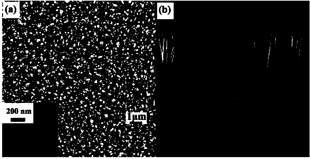
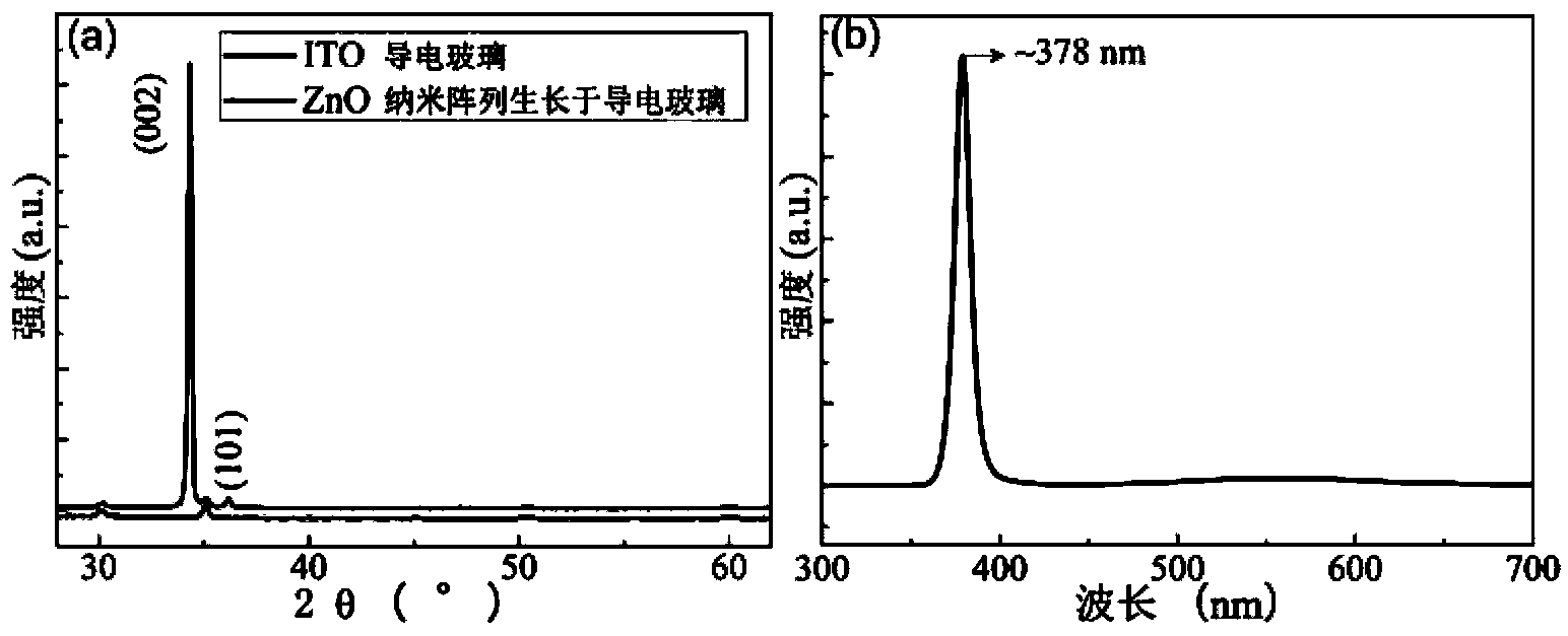
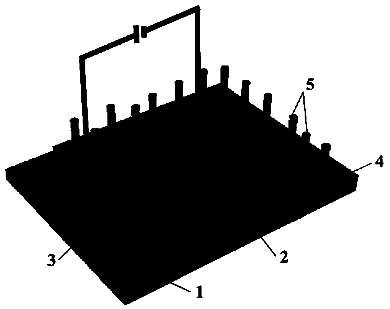
[0027] 1) The ITO conductive glass with a size of 9 mm×12 mm was ultrasonically cleaned with acetone, ethanol and isopropanol in sequence, and dried with nitrogen; 2) A layer with a thickness of 200 μm was grown on the ITO conductive glass by magnetron sputtering. nm ZnO thin film, choose ZnO target material with a purity of 99.999%, RF power supply, sputtering rate of 0.018 nm / s; 3) Dot Ag glue near the center of the ZnO thin film and place it at room temperature for 4 h to make it dry. The diameter of the Ag electrode is 1.8 mm; 4) Cover the surface of the Ag electrode with a layer of polydimethylsiloxane PDMS that has been added with a curing agent and placed at room temperature for 45 minutes, and then heated in an oven at 65°C for 40 minutes to make the PDMS electrode protective layer Curing; 5) Put the obtained substrate into a container filled with 0.05 M growth solution (deionized water, zinc nitrate and hexamethylenetetramine) and grow at 95°C for 14 h. After the...

Embodiment 2

[0030] The ultraviolet detector of this embodiment is basically the same as that of Embodiment 1, the difference is that: the thickness of the ZnO film deposited by magnetron sputtering in step 2) of Embodiment 1 is 225 nm in this embodiment; the growth time in step 5) In this example it is 6 h.

[0031]

Embodiment 3

[0033] The ultraviolet detector of this embodiment is basically the same as that of Embodiment 1, the difference lies in: Step 3) of Embodiment 1 In this embodiment, Pt slurry is dotted on the ZnO thin film to make a Pt electrode.

[0034]


PUM


Abstract

The invention discloses a ZnO nanometer array ultraviolet detector and a manufacturing method of the ZnO nanometer array ultraviolet detector. The structure of the ultraviolet detector is of a metal-semiconductor-metal contact type. The ultraviolet detector sequentially comprises a substrate of ITO conductive glass or FTO conductive glass, a ZnO film, an electrode at the other end and a ZnO nanometer array from bottom to top. The substrate is an electrode at one end; the ZnO film covers the substrate, the electrode at the other end is located in the middle position of the ZnO film, and the ZnO nanometer array is arranged on the periphery of the electrode at the other end; the area of the electrode at the other end is 10%-12% of the total area of the substrate. The manufacturing method comprises the following steps: firstly, performing sputtering on the substrate through magnetic control to produce a layer of ZnO film, secondly, installing electrodes on the ZnO film and leading out one end of a wire, thirdly, covering the electrodes with PDMS protection layers, fourthly, developing the ZnO nanometer array through a hydrothermal method, finally, scraping off part of ZnO at the edge on one side of a sample so that the substrate of the conductive glass can be exposed, and leading out the other end of the wire. Thus, the ultraviolet detector is obtained. The ultraviolet detector and the manufacturing method of the ultraviolet detector have the advantages of being simple in manufacturing process, easy to operate, low in cost, high in device sensitivity, stable in performance and the like.

Description

technical field [0001] The invention belongs to the technical field of preparation of nanometer materials and nanometer functional devices, and relates to a ZnO nanometer array ultraviolet detector and a manufacturing method of the ultraviolet detector. [0002] Background technique [0003] Ultraviolet detectors are widely used in scientific research, military, space, environmental protection and many industrial fields, such as ultraviolet light monitors in spaceships, ozone layer solar ultraviolet monitoring, thermal background flame detection, exhaust gas monitoring, etc.; can also be used in medicine, biology etc.; in daily life, it can also be used as a UV-A (230~400nm) and UV-B (280~320nm) ultraviolet meter for personal use in rich ultraviolet environments such as beaches and mountains. [0004] ZnO is a wide bandgap direct bandgap compound semiconductor material with a bandgap width of about 3.37 eV and an exciton binding energy as high as 60 meV. The ultraviolet st...

Claims


Application Information

Patent Timeline
Patent Type & Authority Applications(China)
IPC IPC(8): H01L31/0224H01L31/18H01L31/09
CPCY02P70/50
Inventor 张跃衣芳廖庆亮黄运华闫小琴
Owner UNIV OF SCI & TECH BEIJING
Why Eureka
Try Eureka