LED epitaxial growth method

A technology of epitaxial growth and growth process, which is applied in the new field of LED epitaxial growth, can solve problems such as changing the effective bandgap width, reducing device stability, and reducing quantum efficiency, so as to reduce the change of the forbidden band width and improve the quantum efficiency , the effect of reducing height

Inactive Publication Date: 2015-06-24
西安利科光电科技有限公司
View PDF5 Cites 2 Cited by
  • Summary
  • Abstract
  • Description
  • Claims
  • Application Information

AI Technical Summary

Problems solved by technology

The polarization electric field generated by this polarization effect will not only change the effective bandgap width, but also make the LED light emission wavelength blue shift under the condition of high current injection, reduce the stability of the device, and also make the hole electron space distribution in the quantum well The wave function is separated, resulting in a decrease in the quantum efficiency of the LED and a decrease in the luminous intensity

Method used


Image

  • LED epitaxial growth method
  • LED epitaxial growth method
  • LED epitaxial growth method

Examples


Embodiment 1

[0026] Embodiment one (the present invention)

[0027] 1. Put the cleaned sapphire substrate into the MOCVD equipment and bake it at 1100°C for 10 minutes.

[0028]2. A low-temperature GaN layer with a thickness of 10 nm is grown at a cooling temperature of 620° C., and the growth pressure is 500 torr.

[0029] 3. Raise the temperature to 1165°C to grow an undoped u-GaN layer with a thickness of 1.5um, and the growth pressure is 200torr.

[0030] 4. Raise the temperature to 1170° C. to grow a silane-doped n-GaN layer with a thickness of 2.0 μm and a growth pressure of 200 torr.

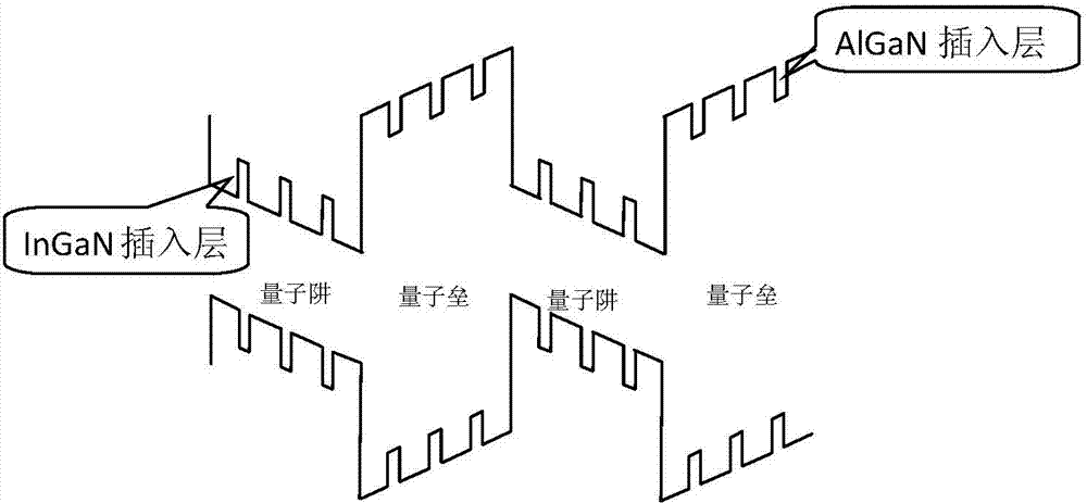
[0031] 5. Switch the carrier gas from hydrogen to nitrogen, and the pressure is 200torr. Cool down to 1065°C, grow In with a thickness of 1nm 0.42 Ga 0.58 N quantum well layer, regrown In with a thickness of 0.8nm 0.15 Ga 0.85 The N insertion layer grows for two cycles in this way, and finally grows In with a thickness of 1nm 0.42 Ga 0.58 N quantum well layer to complete quantum well growth; (...

Embodiment 2

[0038] Embodiment 2 (traditional solution)

[0039] 1. Put the cleaned sapphire substrate into the MOCVD equipment and bake it at 1100°C for 10 minutes.

[0040] 2. A low-temperature GaN layer with a thickness of 10 nm is grown at a cooling temperature of 620° C., and the growth pressure is 500 torr.

[0041] 3. Raise the temperature to 1165°C to grow an undoped u-GaN layer with a thickness of 1.5um, and the growth pressure is 200torr.

[0042] 4. Raise the temperature to 1170° C. to grow a silane-doped n-GaN layer with a thickness of 2.0 μm and a growth pressure of 200 torr.

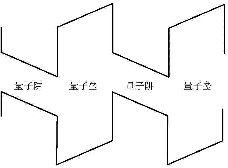
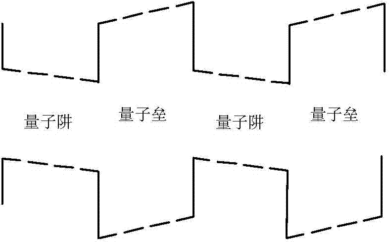
[0043] 5. Switch the carrier gas from hydrogen to nitrogen, the pressure is 200torr, and grow In 0.42 Ga 0.58 N / Al 0.1 Ga 0.9 N multiple quantum well layer. The specific method is: lower the temperature to 1065°C, and grow In with a thickness of 3nm. 0.42 Ga 0.58 N quantum well layer; then raise the temperature to 1175°C, and grow Al with a thickness of 10nm 0.1 Ga 0.9 The N quantum barrier la...


PUM

PropertyMeasurementUnit
Thicknessaaaaaaaaaa
Thicknessaaaaaaaaaa
Thicknessaaaaaaaaaa

Abstract

The invention provides a novel LED epitaxial growth method. LED internal quantum efficiency can be effectively improved, LED light emitting intensity is improved, and LED light emitting wave length stability is improved. The LED epitaxial growth method includes the steps that a low-temperature buffer layer, a non-doping high-temperature GaN layer, a Si-doping high-temperature GaN layer, an InxGa1-xN / AlyGa1-yN multi-quantum-well layer, a p-AlGaN layer and a Mg-doping p-GaN layer grow sequentially, wherein the inequations 0<=x<=1 and 0<=y<=1 are satisfied; multiple InaGa1-aN thin layers with the smaller lattice constants are interposed in the InxGa1-xN quantum well growth process during at least one period, wherein the inequation 0<=a<x<=1 is satisfied; multiple AlbGa1-bN thin layers with the larger lattice constants are interposed in the AlyGa1-yN quantum well growth process during at least one period, wherein the inequation 0<=b<y<=1 is satisfied.

Description

Technical field: [0001] The invention belongs to the preparation technology of semiconductor electronic devices, in particular to a new LED epitaxial growth method. Background technique: [0002] In recent years, III-nitrides have been widely used in optoelectronic devices such as light-emitting diodes, lasers, and detectors, and have shown good development prospects. GaN-based light-emitting diodes (LEDs) are the most promising solid-state light sources for general lighting in the future, and their wide application will save a lot of energy. The usual LED epitaxial growth process is: using MOCVD equipment, first grow a buffer buffer layer on a sapphire substrate, then grow a layer of undoped high-temperature GaN layer, and then grow a layer of Si-doped high-temperature n-GaN to provide composite electrons, and then grow In x Ga 1-x N / Al y Ga 1-y N (0≤x≤1, 0≤y≤1) multi-quantum well layer, then grow a p-AlGaN layer, and finally grow a Mg-doped p-GaN layer to provide hole...

Claims


Application Information

Patent Timeline
IPC IPC(8): H01L33/00H01L33/06H01L33/28
CPCH01L33/0066H01L33/0075H01L33/06H01L33/28
Inventor 商毅博
Owner 西安利科光电科技有限公司
Why Eureka
Try Eureka