PCB glue removing method in mode of vertically depositing copper wires

A PCB board and sinking copper technology, which is applied in the field of PCB board manufacturing, can solve the problems of low glue removal output and production efficiency, and achieve the effects of improved glue removal production efficiency, low equipment cost, and low equipment cost

Inactive Publication Date: 2015-06-24
SHENZHEN SUNTAK MULTILAYER PCB
4 Cites 21 Cited by

AI-Extracted Technical Summary

Problems solved by technology

[0007] The purpose of the present invention is to provide a method for removing glue on vertical copper wires of PCB boards, aiming to...

Method used

The deglue method of PCB board vertical sinking copper wire provided by the present invention, it only increases the second expansion cylinder and the second deglue cylinder, thereby making high TG board expand for the second time and desmear for the second time can It is carried out separately in the second expansion cylinder and the second glue removal cylinder respectively. At the same time, the next batch of high TG boards can be expanded for the first time and the second glue removal cylinder respectively in the first expansion cylinder and the first glue removal cylinder. One-time glue removal does not affect each other, and the high TG board can be continuously and uninterruptedly removed. Since the equipment cost of the second expansion cylinder and the second glue removal...

Abstract

The invention discloses a PCB glue removing method in the mode of vertically depositing copper wires, and the method is applicable to a PCB manufacturing technology. The method includes the steps of board feeding, expanding, first water washing, first glue refuse removing, second water washing, first neutralizing, third water washing, second expanding, fourth water washing, second glue refuse removing and fifth water washing. According to the method, only a second expanding position and a second glue removing position are added, so that second expanding and second glue refuse removing of high-TG boards can be conducted in a second expanding cylinder and a second glue removing cylinder separately and respectively, the situation that in the prior art, the expanding cylinders are left unused after first glue refuse removing is conducted, and glue removing can be conducted on the next batches of the high-TG boards only after second expanding and second glue refuse removing are conducted can be avoided, glue removing can be conducted on the high-TG boards continuously, due to the fact that the equipment costs of the second expanding cylinder and the second glue removing cylinder are lower, on the basis of the lower equipment cost, the high-TG board glue removing yield is greatly increased, and production efficiency is greatly improved.

Application Domain

Conductive pattern polishing/cleaningPrinted element electric connection formation

Technology Topic

Image

  • PCB glue removing method in mode of vertically depositing copper wires
  • PCB glue removing method in mode of vertically depositing copper wires
  • PCB glue removing method in mode of vertically depositing copper wires

Examples

  • Experimental program(1)

Example Embodiment

[0043] In order to make the objectives, technical solutions and advantages of the present invention clearer, the following further describes the present invention in detail with reference to the accompanying drawings and embodiments. It should be understood that the specific embodiments described herein are only used to explain the present invention, but not to limit the present invention.
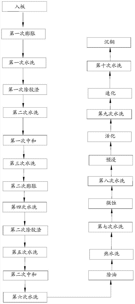
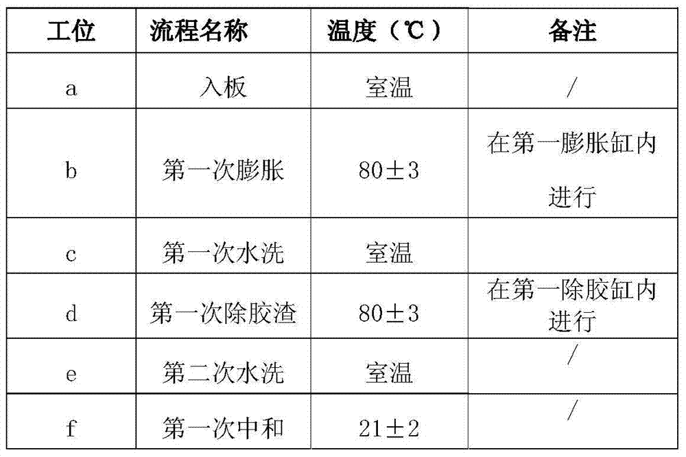
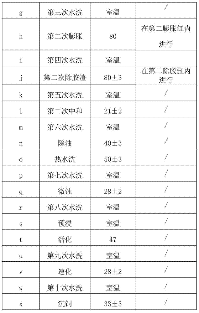
[0044] Such as figure 1 As shown, a method for removing glue from a vertical sinking copper wire of a PCB board provided by an embodiment of the present invention is used to remove the drilling residue remaining on the hole wall after the PCB board is drilled, and includes the following steps:
[0045] a. Load the board, that is, prepare the PCB board that needs to be glued. The TG value of the PCB board is ≥170°C, which is a high TG board;
[0046] b. The first expansion, that is, the PCB board is immersed in a chemical solution containing ether and phosphoric acid, and the immersion time is 8-9 minutes to break the polymer chain of the pore wall resin, thereby preparing for the subsequent process;
[0047] c. The first water washing is to clean the PCB board after the first expansion with running water. Because the running water is in a flowing state, the washed dirt can be taken away immediately to avoid secondary pollution and make the PCB board The cleaning effect is better, and the cleaning efficiency is also higher;
[0048] d. Desmear for the first time, that is, immerse the PCB board after the first washing with a solution containing potassium permanganate and sodium hydroxide. The immersion time is 12-16 minutes to remove part of the polymer The resin molecules with broken chains dissolve;
[0049] e. The second water washing, that is, the PCB board after the first de-smearing is cleaned with running water to remove the surface dirt of the PCB board;
[0050] f. The first neutralization, that is, neutralize the manganese residues remaining on the pore wall with the neutralizer containing sulfuric acid and hydrogen peroxide. The neutralization time is 2 to 3 minutes;
[0051] g. The third water washing, that is, the PCB board after the first neutralization is cleaned with running water, so that the dirt attached to the PCB board is washed away;
[0052] Wherein, the first expansion is carried out in a first expansion cylinder, the first desmearing is carried out in the first desmearing cylinder, and the method for removing glue of the vertical copper sinking wire of the PCB board further includes: After the third water wash, it also includes the following steps:
[0053] h. The second expansion, that is, the PCB board after the third water washing is put into the expansion tank containing the chemical solution containing ether and phosphoric acid again, and the immersion time is 8-9 minutes to further improve the hole wall The polymer chain of the resin is broken;
[0054] i. The fourth water washing, that is, washing the PCB board after the second expansion with running water to remove the dirt attached to the PCB board;
[0055] j. Desmear the second time, that is, use the solution containing potassium permanganate and sodium hydroxide to impregnate the residual drilling residue on the hole wall of the PCB board for the second time, and the immersion time is still 12-16 Minutes, dissolve the resin molecules with broken polymer chains remaining on the hole wall, thereby removing the glue residue;
[0056] k. The fifth water wash, that is, use running water to clean the PCB board after the second de-smearing;
[0057] Wherein, the second expansion is performed in a second expansion cylinder, and the second degreasing is performed in a second degreasing cylinder.
[0058] The invention provides a method for removing glue from a vertical sinking copper wire of a PCB board, which only adds a second expansion cylinder and a second glue removal cylinder, so that the second expansion of the high TG board and the second desmear can be respectively The second expansion cylinder and the second degumming cylinder are carried out separately. At the same time, the next batch of high TG boards can simultaneously perform the first expansion and the first degumming in the first expansion cylinder and the first degumming cylinder. The glue residue does not affect each other, and can continuously and uninterruptedly remove glue on the high TG board. Since the equipment cost of the second expansion cylinder and the second glue removal cylinder is lower than the cost of the entire chemical glue removal production line, the present invention On the basis of lower equipment costs, the production efficiency of degumming for high TG boards has been greatly improved, and the output has also been greatly improved; at the same time, due to the addition of the second expansion cylinder and the second degumming cylinder, the original The equipment has no influence, so it does not affect the degumming of low TG boards and medium TG boards, so that various boards of low TG boards, medium TG boards and high TG boards can be degummed efficiently.
[0059] Specifically, after the fifth water washing, the following steps are further included:
[0060] 1. The second neutralization is to use a neutralizer containing sulfuric acid and hydrogen peroxide to neutralize the manganese residues remaining on the pore wall of the second desmearing residue to remove the remaining manganese compounds. Neutralization time 2 to 3 minutes;
[0061] m. The sixth water washing, that is, the PCB board after the second neutralization is washed with running water;
[0062] o. Wash with hot water, use hot water to clean the PCB board after the degreasing step;
[0063] p. The seventh water washing, that is, washing the PCB board after the hot water washing step with running water;
[0064] q. Micro-etching, that is, using a micro-etching agent containing sodium persulfate and sulfuric acid to roughen the copper surface of the PCB board after the seventh water washing to increase the bonding force between the substrate copper and the electroplated copper;
[0065] r. The eighth water wash, that is, use running water to clean the PCB board after the micro-etching step;
[0066] s. Pre-soaking, that is, immersing the PCB board after the eighth water washing step with a solution containing sodium bisulfate to prevent the residual water on the PCB board from being directly carried into the next process;
[0067] t. Activation, that is, soaking the PCB board after the prepreg step with a solution containing sodium bisulfate and colloidal palladium, so that a layer of colloidal palladium is adsorbed on the hole wall;
[0068] u. The ninth water washing, that is, washing the activated PCB board with running water;
[0069] v. Speeding, that is, using a solution containing fluoroboric acid to remove the colloidal palladium adsorbed on the pore wall of the PCB board after the ninth water washing;
[0070] w. The tenth water washing, that is, washing the accelerated PCB board with running water;
[0071] x. Copper deposition, that is, using a solution containing copper ions, sodium hydroxide, formaldehyde, and a complexing agent, deposit a 0.3-0.8um copper layer on the hole wall of the PCB board after the tenth water washing.
[0072] Please refer to Table 1 for a detailed description of each step and working temperature:
[0073]
[0074]
[0075] Table 1
[0076] Further, the temperature of the solution in the expansion cylinder during the second expansion is 80±3, and the solution temperature is preferably 80°C, and the expansion effect is the best at this time.
[0077] Further, the water temperature from the first washing to the eleventh washing is the natural temperature of water at room temperature.
[0078] Further, during the second de-smearing, the temperature of the solution in the second de-gluing tank is 80±3, wherein the solution temperature is preferably 80°C. After testing, the de-gluing effect at this time Better.
[0079] Further, the solution temperature of the neutralizer in the first neutralization and the second neutralization step is 21±2 degrees, and the neutralization effect is better when the solution is 21 degrees.
[0080] Further, the temperature of the alkaline solution in the degreasing step is 40±3 degrees. Preferably, when the temperature of the alkaline solution is 40 degrees, the degreasing effect is better.
[0081] Further, the temperature of the hot water in the hot water washing step is 50±3 degrees. When it is 50 degrees, the temperature can effectively remove stains and avoid excessive temperature that may affect the performance of the PCB board. .
[0082] The above descriptions are only preferred embodiments of the present invention, and are not intended to limit the present invention. Any modification, equivalent replacement or improvement made within the spirit and principle of the present invention shall be included in the protection of the present invention. Within range.

PUM

no PUM

Description & Claims & Application Information

We can also present the details of the Description, Claims and Application information to help users get a comprehensive understanding of the technical details of the patent, such as background art, summary of invention, brief description of drawings, description of embodiments, and other original content. On the other hand, users can also determine the specific scope of protection of the technology through the list of claims; as well as understand the changes in the life cycle of the technology with the presentation of the patent timeline. Login to view more.

Similar technology patents

Waste gas incinerator

ActiveCN102721071AReduce equipment costsImprove cost performance and market competitivenessIncinerator apparatusProcess engineeringCombustion chamber
Owner:常州市鼎龙环保设备有限公司

Classification and recommendation of technical efficacy words

Why Eureka
Try Eureka