Method of manufacturing a display device

a display device and manufacturing method technology, applied in the field of manufacturing methods of display devices, can solve the problems of increasing equipment cost and maintenance costs, increasing the size of processing devices, and increasing the cost of air discharging systems, so as to reduce equipment costs, simplify air discharging systems, and suppress energy

Inactive Publication Date: 2005-04-28
SEMICON ENERGY LAB CO LTD
View PDF36 Cites 61 Cited by
  • Summary
  • Abstract
  • Description
  • Claims
  • Application Information

AI Technical Summary

Benefits of technology

[0011] The above-descried means which emits droplets, or the above-described gas phase reaction process is designed to be carried out under atmospheric pressure or in the vicinity of atmospheric pressure. On that account, it becomes possible to omit an air discharging system for realizing a vacuum or reduced pressure status in a process chamber, which is required in a conventional vacuum process. Therefore, it is possible to simplify the air discharging system which grows in size based on size growing of a substrate, and it is possible to reduce equipment cost. Also, in compliance with this, it becomes possible to suppress energy etc. for discharging air, which results in reduction of environmental burdens. Further, since it is possible to omit time for air discharge, tact time is improved, so that it becomes possible to carry out production of a substrate more effectively.

Problems solved by technology

In order to lay out the equipment, a space for the air discharging system becomes necessary outside the processing apparatus, and costs for the same become also necessary.
Further, since it is also necessary to mount equipment of the air discharging system to the processing apparatus itself, a size of the processing device becomes larger as compared to a thing on which the air discharging system is not mounted.
Further, also in a cost phase, equipment cost and maintenance cost etc. of the air discharging system mount up.
In addition, also in a case of replacing the chamber with gas such as nitrogen, a much more amount of gas becomes necessary because of volume increase of the chamber, which has an influence on production cost.
Further, in connection with size growing of the substrate, huge running costs are required for power supply etc., and therefore, it results in increase of environment burdens.
In short, a most part of a material is to be thrown away, which not only has an influence on production cost, but also invites increase of environmental burdens.

Method used


Image

  • Method of manufacturing a display device
  • Method of manufacturing a display device
  • Method of manufacturing a display device

Examples


embodiment 1

[0133] (Embodiment 1)

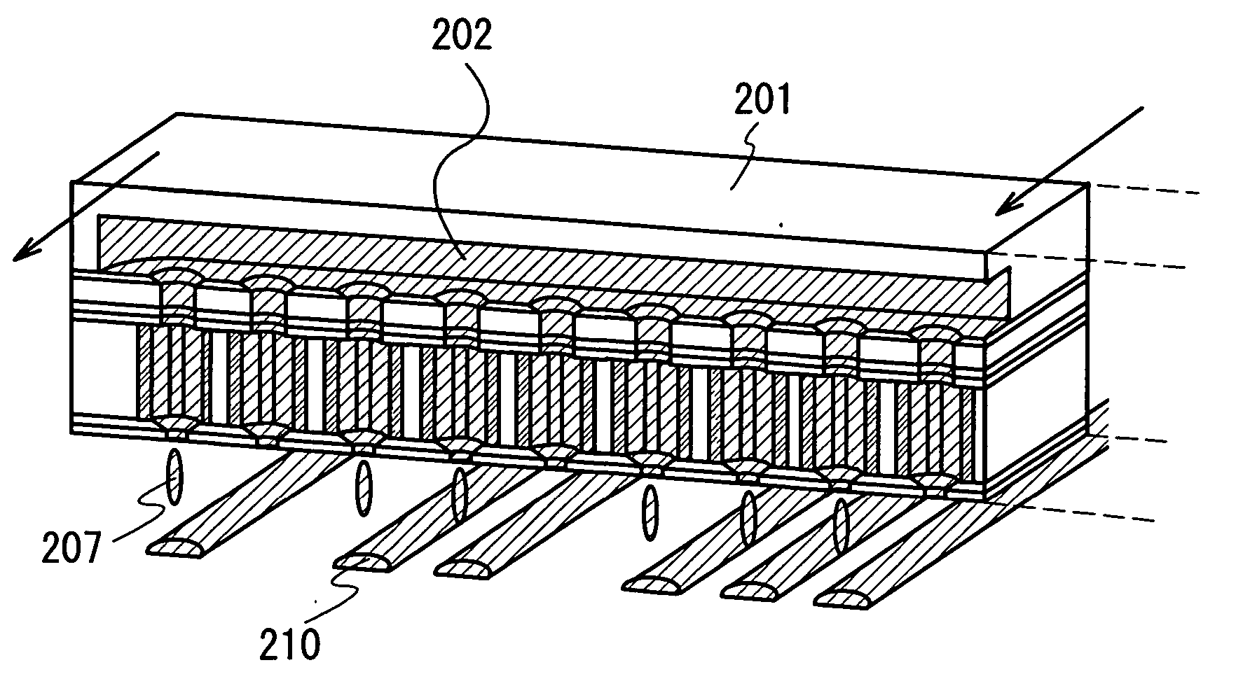
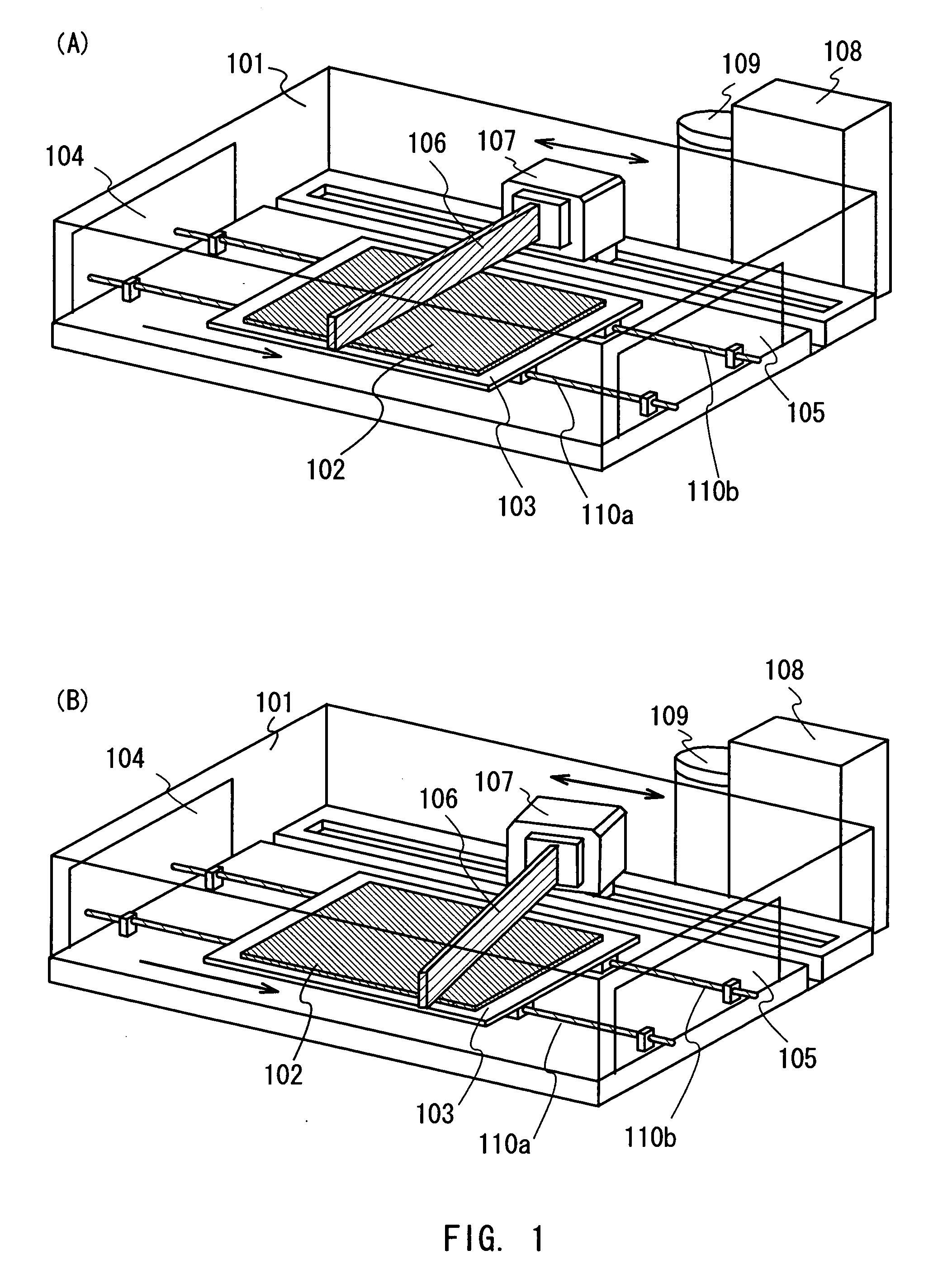
[0134] A manufacturing method of a display device of the invention, which uses a droplet emitting apparatus which has a droplet emitting head in which a plurality of droplet emitting holes are disposed in a line form, and a plasma processing apparatus which has plasma generating means under atmospheric pressure or the vicinity of atmospheric pressure, will be explained. Hereinafter, with reference to the drawings, embodiments of the invention will be described. An embodiment 1 of the invention is a manufacturing method of a channel stop type thin film transistor (TFT).

[0135] On a substrate 2001 to be processed, which uses various materials such as glass, quartz, semiconductor, plastic, plastic film, metal, glass epoxy resin, and ceramic, a composition having publicly known electric conductivity is emitted on a necessary place, by use of a line form droplet emitting apparatus of the invention, and thereby, a gate electrode and wiring 2002, a capacitance electrod...

embodiment 2

[0152] (Embodiment 2)

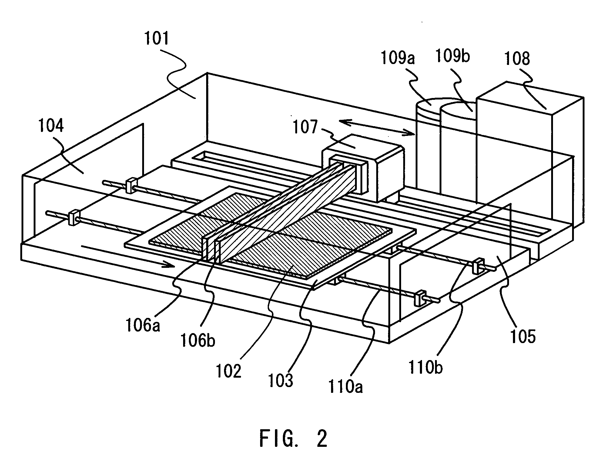
[0153] A manufacturing method of a display device of the invention, which uses the above-described droplet emitting apparatus which has the droplet emitting head in which the circular droplet emitting holes are disposed in a line form, and the plasma processing apparatus which has the plasma generating means under atmospheric pressure or the vicinity of atmospheric pressure, will be explained. In this embodiment, it is characterized by manufacturing a thin film transistor (TFT), without using a photolithography process which uses a resist mask at all. Hereinafter, with reference to the drawings, an embodiment of the invention will be explained. An embodiment 2 of the invention is a manufacturing method of a channel stop type thin film transistor (TFT).

[0154] On a substrate 3001 to be processed, which uses various materials such as glass, quartz, semiconductor, plastic, plastic film, metal, glass epoxy resin, and ceramic, a composition having publicly known elec...

embodiment 3

[0171] (Embodiment 3)

[0172] A manufacturing method of a display device of the invention, which uses a droplet emitting apparatus which has a droplet emitting head in which a droplet emitting hole is disposed in a line form, and a plasma processing apparatus which has plasma generating means under atmospheric pressure or the vicinity of atmospheric pressure, will be explained. Meanwhile, either a line form droplet emitting apparatus and a dot form droplet emitting apparatus may be used as the droplet emitting apparatus. Hereinafter, with reference to FIG. 26 to FIG. 27, an embodiment of the invention will be described. This embodiment is a manufacturing method of a channel etch type thin film transistor (TFT).

[0173] Firstly, on a substrate 3101, a thin film (not shown in the figure) including Ti is film-formed. Here, a Ti thin film with 5 nm or less was film-formed on a glass substrate, but it is not limited to this. By film-forming the thin film including Ti, it is possible to heig...


PUM


Abstract

In a wiring manufacturing process which uses conventional photolithography, most of resist and wiring material, or process gas which is necessary at the time of plasma processing, etc. is wasted. Also, since air discharging means such as a vacuum equipment is necessary, an entire apparatus grows in size, and therefore, it has been a problem that production cost increases with growing in size of a processing substrate. In this invention, applied is such means that droplets are used for resist and wiring material, and they are emitted directly to a necessary place on the substrate in a line form or a dot form, to draw a pattern. Also, applied is means which carries out a gas reaction process such as ashing and etching, under atmospheric pressure or the vicinity of atmospheric pressure.

Description

TECHNICAL FIELD [0001] This invention relates to a manufacturing method of a display device which uses droplet emitting means and an atmospheric pressure plasma processing method. BACKGROUND ART [0002] Manufacture of circuit patterns of thin film transistors (TFT) etc. which are included in a display device typified by a liquid crystal display device (LCD) and a light-emitting display device (EL(Electro-Luminescence)) display device) has used a vacuum process which is carried out in such a status that an inside of a processing apparatus is in reduced pressure or vacuum, and a photolithography process in which a mask, which comprises a (photo) resist, is manufactured by a light exposure apparatus and an unnecessary portion is removed by etching. (See, Patent Document 1) [0003] (Patent Document 1) JP-A-2002-359246 publication [0004] The vacuum process requires air discharging means for forming a vacuum or reducing a pressure of a process chamber for carrying out film-formation, etchin...

Claims


Application Information

Patent Timeline
Patent Type & Authority Applications(United States)
IPC IPC(8): H01L21/288H01L21/77H01L21/84
CPCH01L21/288H01L27/1292H01L51/0022H10K71/611H01L27/1214H01L21/31138G03F7/2018
Inventor YAMAZAKI, SHUNPEIHOSOYA, KUNIO
Owner SEMICON ENERGY LAB CO LTD
Why Eureka
Try Eureka