Method for polishing single silicon chip

A technology of silicon single wafer and flow tank, which is applied to surface polishing machine tools, grinding/polishing equipment, abrasives, etc., can solve problems such as waste and increase production costs, reduce flatness variation, stabilize the shape of the large disk, and improve Effect of polish removal rate

Inactive Publication Date: 2015-07-01
JINGHUA ELECTRONICS MATERIAL
View PDF0 Cites 0 Cited by
  • Summary
  • Abstract
  • Description
  • Claims
  • Application Information

AI Technical Summary

Problems solved by technology

In the prior art, the local flatness STIR (SBIR) of silicon single crystal polished wafers is ≤1μm15*15mm 2 The yield rate is only 75%, which not only wastes a lot, but also increases the production cost

Method used


Image

  • Method for polishing single silicon chip
  • Method for polishing single silicon chip

Examples


Embodiment 1

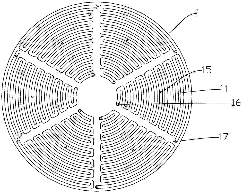
[0020] Such as figure 1 As shown in the silicon single wafer polishing method, a silicon wafer is used to polish a large plate 1 , and a flow groove 11 is arranged on the surface of the large plate 1 . The circulation groove 11 extends radially from the edge of the large disk 1 to the center of the circle and is arranged around the circumference. There are 6 circulation grooves 11 arranged along the circumferential direction. A liquid outlet 15 , a first liquid inlet 16 , and a second liquid inlet 17 are arranged in each flow tank 11 . The liquid outlet 15 is located at half the radius from the center of the circle. The first liquid inlet 16 is located near the center of the circle; the second liquid inlet 17 is located near the edge of the large plate 1 . The cooling water enters the circulation groove 11 from the liquid outlet 15 and is divided into two paths, one path flows toward the center of the circle and then enters the first liquid inlet 16 ; the other path flows t...

Embodiment 2

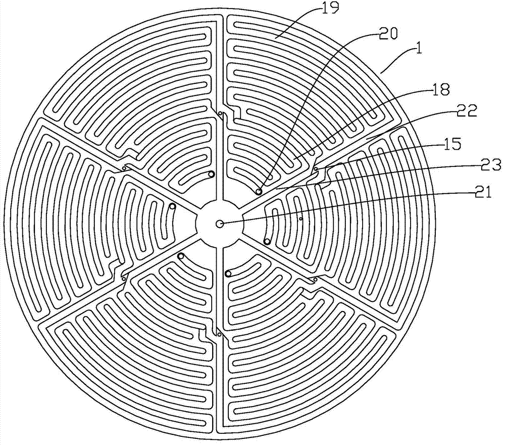
[0022] Such as figure 2 As shown, in the silicon single wafer polishing method, a silicon wafer is used to polish a large disk 1, and a flow groove is arranged on the surface of the large disk 1. The flow grooves include 6 inner ring flow grooves 18 and 6 outer ring flow grooves 19; an outer ring flow groove 19 is arranged on the periphery of an inner ring flow groove 18; a liquid outlet 15 is provided on the surface of the large plate 1; the liquid outlet 15 is located at At half the radius from the center of the circle; each liquid outlet 15 communicates with an inner ring flow groove 18 and an outer ring flow groove 19 at the same time. A third liquid inlet 20 is arranged on the surface of the large plate 1, and the third liquid inlet 20 is arranged in the inner ring flow groove 18 and is close to the center of the circle. A fourth liquid inlet 21 is provided at the center of the large plate 1 . The outer ring flow groove 19 communicates with the liquid outlet 15 through...


PUM


Abstract

The invention discloses a method for polishing a single silicon chip. The method is characterized in that the single silicon chip is cooled by the aid of water in polishing procedures, and the temperature of the water ranges from 20 DEG C to 30 DEG C. The method for polishing the single silicon chip has the advantages that the temperature of the cooling water is approximately equal to the polishing temperature, accordingly, the polishing temperature can be quickly increased, the polishing removal speed can be improved, and the low-temperature polishing procedures can be shortened; the shape of a large plate of a polishing machine can be stabilized, and variation of the flatness of machined products due to change of the shape of the large plate can be reduced; the site flatness STIR (site total indicator reading) [SBIR (site flatness back ideal range)] is lower than or equal to 1 micrometer at the condition of 15*15 mm<2>, and the yield is higher than 95%.

Description

technical field [0001] The invention relates to a silicon single wafer polishing method. Background technique [0002] The purpose of polishing the surface of the silicon wafer is to remove the tiny defects left on the surface by the previous sequence (slicing, grinding, etc.), the stress damage layer on the surface, and the impurities such as various metal ions on the surface to obtain The clean and bright "mirror surface" with local flatness and extremely low surface roughness meets the technical requirements for silicon wafers for the preparation of various microelectronic devices. [0003] The surface polishing of silicon wafers is a key process in silicon wafer processing, and its processing accuracy directly affects the technical indicators such as the performance and pass rate of IC chips. [0004] Surface local roughness (STIR) of silicon single crystal polished wafers is one of the key parameters to confirm the quality of polished wafers, and STIR, as a key paramet...

Claims


Application Information

Patent Timeline
Patent Type & Authority Applications(China)
IPC IPC(8): B24B29/02
CPCB24B29/02B24D13/18
Inventor 林涛邹晓明周小勇方正华陈建纲
Owner JINGHUA ELECTRONICS MATERIAL
Why Eureka
Try Eureka