NEA electron source for vertically emitting AlGaAs/GaAs nanowires

A technology of vertical emission and electron source, applied in the direction of photoemission cathode, circuit, discharge tube, etc., to achieve the effect of high vertical emission efficiency at the top, sufficient photon absorption, and suppression of side photoemission

Inactive Publication Date: 2015-07-01
EAST CHINA UNIV OF TECH
View PDF6 Cites 16 Cited by
  • Summary
  • Abstract
  • Description
  • Claims
  • Application Information

AI Technical Summary

Problems solved by technology

In 2010, Maite Volatier from the University of Sherbrooke, Canada, used inductively coupled plasma etching technology to prepare AlGaAs / GaAs nanowire waveguide structures with variable bandgap from 0 to 100% Al composition; in 2012, Anuj GaAs nanowire arrays were prepared by combining nanosphere etching and selective area metal-organic chemical vapor deposition by R.Madaria et al. In 2014, Paola Prete et al. of the Italian Institute of Microelectronics and Microsystems grew AlGaAs / GaAs cores by metal-organic chemical vapor deposition. -nanowire array with shell structure; at the same time, researchers at home and abroad have also explored its application in optical waveguides, light-emitting diodes, etc., but there has been no relevant report on the field of photoelectric emission electron sources

Method used


Image

  • NEA electron source for vertically emitting AlGaAs/GaAs nanowires
  • NEA electron source for vertically emitting AlGaAs/GaAs nanowires
  • NEA electron source for vertically emitting AlGaAs/GaAs nanowires

Examples


Embodiment Construction

[0036] In order to make the technical means, creative features, goals and effects achieved by the present invention easy to understand, the present invention will be further described below in conjunction with specific illustrations.

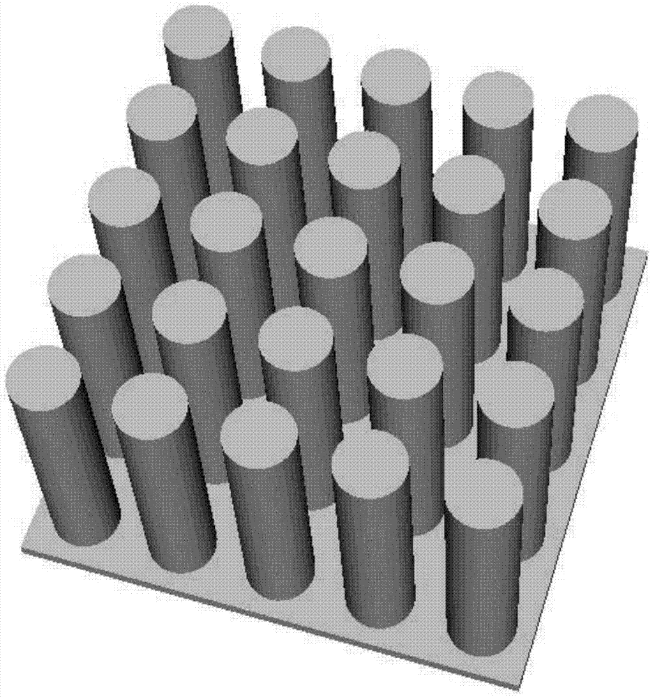
[0037] see figure 1 A kind of NEA electron source that vertically emits AlGaAs / GaAs nanowires. The variable bandgap AlGaAs / GaAs nanowire arrays are arranged periodically and neatly. When light is incident, the light is continuously absorbed in the variable bandgap AlGaAs / GaAs nanowire arrays. , reflection, and refraction until most of the light is absorbed, since the variable bandgap AlGaAs / GaAs nanowires have a built-in electric field along the vertical direction, most of the photoelectrons drift to the top of the nanowires under the action of the built-in electric field, and finally from The top GaAs emitter layer emits into vacuum, enabling vertical photoemission.

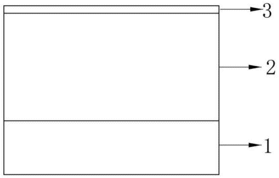
[0038] A method for preparing a NEA electron source for vertically emitting ...


PUM


Abstract

The invention provides an NEA electron source for vertically emitting AlGaAs/GaAs nanowires. A p type GaAs is taken as a substrate layer, a variable-band gap AlGaAs emission layer of which the Al component is linearly and gradually reduced to zero from high to low, and a GaAs emission layer are orderly grown on the GaAs substrate layer, next, a variable-band gap AlGaAs/GaAs nanowire array emission layer is obtained by use of a reactive ion etching technique, and then Cs/O excitation is performed in an ultrahigh vacuum system so as to form a Cs-O activation layer on the variable-band gap AlGaAs/GaAs nanowire array emission layer; in addition, a built-in electric field is formed on the variable-band gap AlGaAs/GaAs nanowire array emission layer in the vertical direction, and the photoelectrons in the nanowires are controlled to directionally drift and be emitted by use of the built-in electric field, so that the photoelectric emission of the side surface can be effectively inhibited, and therefore, the application of the variable-band gap AlGaAs/GaAs material is expanded; the nanowire array structure is capable of improving the photoelectric emission efficiency.

Description

technical field [0001] The invention relates to the technical field of vacuum photoelectric emission materials, in particular to a NEA electron source for vertically emitting AlGaAs / GaAs nanowires. Background technique [0002] Negative electron affinity (NEA) electron source is a photocathode material that converts incident light into electron emission by using the external photoelectric effect. Negative electron affinity GaAs electron source has high quantum efficiency, small dark emission, and emitted electron energy It has many advantages such as concentrated angular distribution, high spin polarizability of emitted electrons, high emission current density, and uniform planar electron emission. It has been widely used in electron accelerators, free electron lasers, and high-end instruments and equipment. [0003] Traditional NEA electron sources are usually made of thin-film materials. However, due to the high reflectivity of thin-film materials, the transport distance o...

Claims


Application Information

Patent Timeline
Patent Type & Authority Applications(China)
IPC IPC(8): H01J1/34H01J9/12
CPCH01J1/34H01J9/12H01J2201/34
Inventor 邹继军万明冯林邓文娟彭新村程滢江少涛王炜路张益军常本康
Owner EAST CHINA UNIV OF TECH
Why Eureka
Try Eureka