Ion implantation method for improving damage caused by hot carrier injection

An ion implantation and implantation damage technology, applied in electrical components, semiconductor/solid-state device manufacturing, circuits, etc., can solve problems such as MOS device failure, energy bond breakage, threshold voltage linear region/saturation region current degradation, etc., to reduce the longitudinal Electric field strength, damage reduction effect

Inactive Publication Date: 2015-07-01
SHANGHAI HUALI MICROELECTRONICS CORP
View PDF4 Cites 0 Cited by
  • Summary
  • Abstract
  • Description
  • Claims
  • Application Information

AI Technical Summary

Problems solved by technology

[0003] Hot carriers will break the energy bond at the interface between the silicon substrate and the silicon dioxide gate oxygen, and generate interface states at the interface between the silicon substrate and the silicon dioxide gate oxygen, resulting in device performance, such as threshold voltage, transconductance, and linearity. The degradation of the current in the region / saturation region will eventually cause the failure of the MOS device

Method used


Image

  • Ion implantation method for improving damage caused by hot carrier injection
  • Ion implantation method for improving damage caused by hot carrier injection
  • Ion implantation method for improving damage caused by hot carrier injection

Examples


Embodiment Construction

[0030] In order to make the content of the present invention clearer and easier to understand, the content of the present invention will be further described below in conjunction with the accompanying drawings. Of course, the present invention is not limited to this specific embodiment, and general replacements known to those skilled in the art are also covered within the protection scope of the present invention. Secondly, the present invention is described in detail by means of schematic diagrams. When describing the examples of the present invention in detail, for the convenience of explanation, the schematic diagrams are not partially enlarged according to the general scale, which should not be used as a limitation of the present invention.

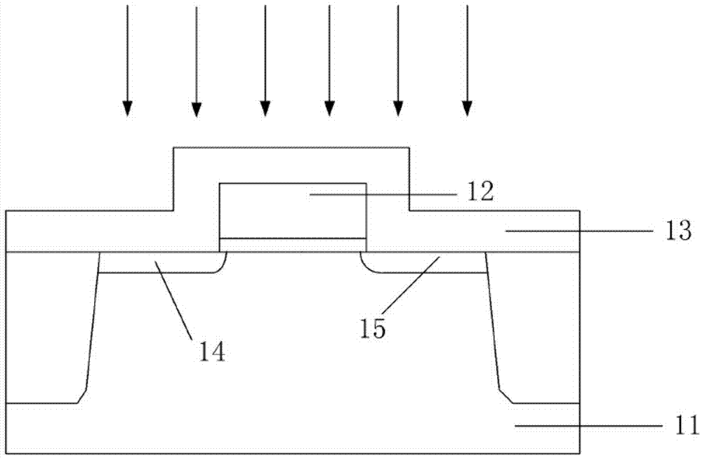
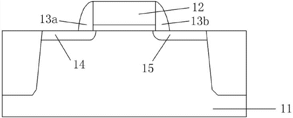
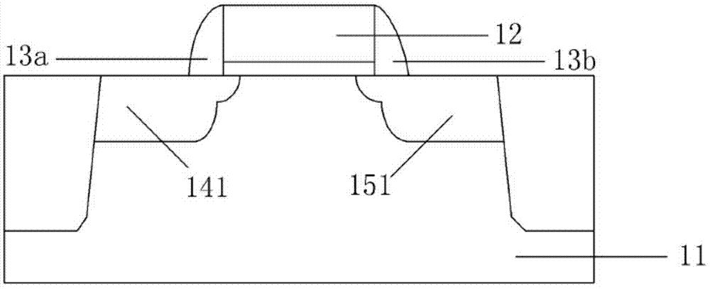
[0031] The above and other technical features and beneficial effects will be combined with the embodiments and the accompanying Figure 4 to Figure 10 The ion implantation method for improving hot carrier injection damage of the prese...


PUM


Abstract

The invention provides an ion implantation method for improving damage caused by hot carrier injection. An ultraviolet processing step is added for a drain area before sidewall etching, so that a sidewall layer above the drain area and a sidewall layer above a source area are of different etching rates, the sectional width of the sidewall of a source is less than that of the sidewall of a drain, distances from doped ions of a drain end to a channel are prolonged, distances from doped ions of a source end to the channel and a substrate are prolonged, longitudinal electric field strength is reduced, and damage of a device caused by hot carrier injection is reduced.

Description

technical field [0001] The invention relates to the field of semiconductor manufacturing, in particular to an ion implantation method for improving hot carrier injection damage. Background technique [0002] The hot carrier effect is an important failure mechanism of MOS (metal oxide semiconductor) devices. With the shrinking of the size of MOS devices, the hot carrier injection effect of the devices becomes more and more serious. Taking a PMOS (P-type metal oxide semiconductor) device as an example, the holes in the channel are accelerated under the action of a high lateral electric field between the drain and source to form high-energy carriers, which collide with the silicon lattice. Generate ionized electron-hole pairs, the electrons are collected by the substrate to form a substrate current, most of the holes generated by the collision flow to the drain, but some holes are injected into the gate under the action of the vertical electric field The formation of gate curr...

Claims


Application Information

Patent Timeline
IPC IPC(8): H01L21/336H01L21/265
CPCH01L29/06H01L29/0607H01L29/66477H01L21/265H01L29/66659H01L29/7835
Inventor 桑宁波李润领关天鹏
Owner SHANGHAI HUALI MICROELECTRONICS CORP
Why Eureka
Try Eureka