Silicon controlled rectifier protection device and forming method thereof

An electrostatic protection and thyristor technology, which is applied in the direction of electric solid-state devices, electrical components, semiconductor devices, etc., can solve problems such as performance improvement, achieve uniform current distribution, increase maintenance voltage, and prevent latch-up effects

Active Publication Date: 2015-07-01
SEMICON MFG INT (SHANGHAI) CORP
View PDF4 Cites 15 Cited by
  • Summary
  • Abstract
  • Description
  • Claims
  • Application Information

AI Technical Summary

Problems solved by technology

[0011] However, the performance of the existing thyristor

Method used


Image

  • Silicon controlled rectifier protection device and forming method thereof
  • Silicon controlled rectifier protection device and forming method thereof
  • Silicon controlled rectifier protection device and forming method thereof

Examples


Embodiment Construction

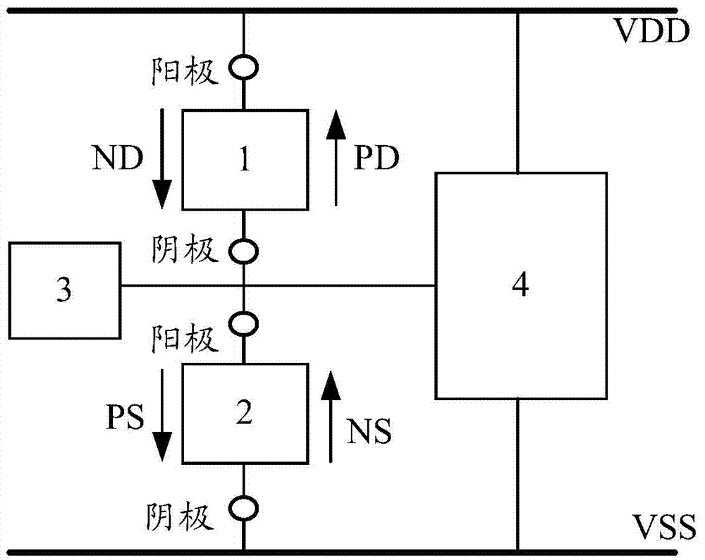
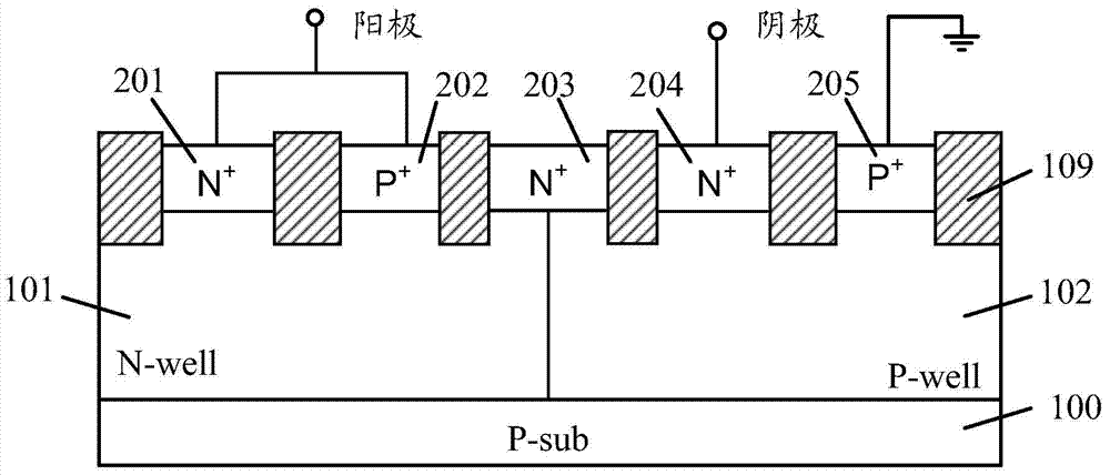
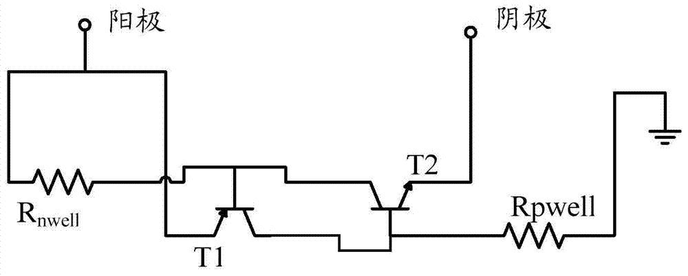
[0041] The trigger voltage of the thyristor electrostatic protection device in the prior art is too high, and the maintenance voltage is too low, which is easy to introduce latch-up effect, which is not conducive to the improvement of the performance of the thyristor electrostatic protection device.

[0042] The invention provides a thyristor electrostatic protection device, which reduces the trigger voltage and increases the maintenance voltage.

[0043] In order to make the above objects, features and advantages of the present invention more comprehensible, specific embodiments of the present invention will be described in detail below in conjunction with the accompanying drawings. When describing the embodiments of the present invention in detail, for convenience of explanation, the schematic diagrams will not be partially enlarged according to the general scale, and the schematic diagrams are only examples, which shall not limit the protection scope of the present invention...


PUM


Abstract

Various embodiments provide SCR ESD protection devices and methods for forming the same. An exemplary device includes a semiconductor substrate having a P-type well region, an N-type well region adjacent to the P-type well region, a first P-type doped region and a first N-type doped region in the P-type well region, and a second N-type doped region and a second P-type doped region in the N-type well region. A first center-doped region and a second center-doped region doped with impurity ions of a same type are located between the first N-type doped region and the second P-type doped region and extend across the P-type well region and the N-type well region. The first center-doped region is located within the second center-doped region, has a doping concentration higher than a doping concentration in the second center-doped region, and has a depth smaller than a depth of the second center-doped region.

Description

technical field [0001] The invention relates to the design field of integrated circuit electrostatic protection circuits, in particular to a thyristor electrostatic protection device and a forming method thereof. Background technique [0002] In the production and application of integrated circuit chips, with the continuous improvement of VLSI process technology, the current CMOS integrated circuit production technology has entered the deep submicron stage, the size of MOS devices is continuously shrinking, and the thickness of the gate oxide layer is increasing. The thinner the MOS device is, the lower the withstand voltage capability of the MOS device is, and the harm of electrostatic discharge (ESD) to integrated circuits becomes more and more significant. Therefore, it becomes particularly important to protect integrated circuits from ESD. [0003] In order to strengthen the ability to protect against static electricity, most of the chip's input and output interface (I / ...

Claims


Application Information

Patent Timeline
IPC IPC(8): H01L27/02H01L29/06
CPCH01L27/0248H01L29/7436H01L29/66393H01L29/0649H01L21/265H01L29/66121H01L29/87H01L27/0262H01L29/0626
Inventor 代萌
Owner SEMICON MFG INT (SHANGHAI) CORP
Why Eureka
Try Eureka