Passivating antireflection film of high PID resistance type polycrystalline cell and preparation process thereof

A preparation process, passivation reduction technology, applied in the field of solar cells, can solve the problems of reduced conversion efficiency, low PID, attenuation, etc., and achieve the effects of reducing reflectivity, improving attenuation characteristics, and increasing short-circuit current

Active Publication Date: 2015-07-01
JIANGSU SHUNFENG PHOTOVOLTAIC TECH CO LTD
View PDF5 Cites 8 Cited by
  • Summary
  • Abstract
  • Description
  • Claims
  • Application Information

AI Technical Summary

Problems solved by technology

[0003] The SiNx passivation anti-reflection coating on the surface of traditional solar polycrystalline cells is almost always due to the low refractive index, which makes the PID attenuation more serious; in order to pursue PID Free in the current market, the main method is to increase the refractive index of the SiNx coating, but the conversion efficiency of the battery is relatively low. The conventional process reduces 1-2%; another method is to use ozone O generated by ultraviolet ionization 3 Oxide the surface of the silicon wafer to generate thinner SiO x layer or PECVD method to directly deposit a layer of SiO on the surface of the silicon wafer x thin film, giving the battery some PID resistance

Method used


Image

  • Passivating antireflection film of high PID resistance type polycrystalline cell and preparation process thereof
  • Passivating antireflection film of high PID resistance type polycrystalline cell and preparation process thereof
  • Passivating antireflection film of high PID resistance type polycrystalline cell and preparation process thereof

Examples


Embodiment 1

[0022] 1). Pretreatment of the original silicon wafer, the pretreatment includes the processes of texturing, diffusion and etching in the battery process;

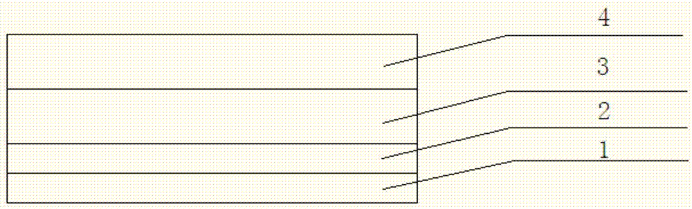
[0023] 2).Oxygen produced by high-voltage ionization or ultraviolet ionization oxygen or compressed air 3 Or free O atoms form a thin layer of dense SiO on the surface of the polysilicon wafer after etching x Layer 1, the refractive index is 1.65, and the film thickness is 0.8nm;

[0024] 3). Use PECVD equipment to coat the remaining film layer on the diffusion surface, cancel the pre-deposition step when coating the film, and coat SiO first x Layer 2, the refractive index is 1.65, and the film thickness is 2nm; then coat high refractive index SiN x Layer 3, the refractive index is 2.20, and the film thickness is 20nm; finally, a single layer of SiN is plated x layer, the refractive index is 2.05, and the film thickness is 60nm;

[0025] 4).Use the traditional battery printing process to print the back electrode, alumi...

Embodiment 2

[0031] 1). Pretreatment of the original silicon wafer, the pretreatment includes the processes of texturing, diffusion and etching in the battery process;

[0032] 2).Oxygen produced by high-voltage ionization or ultraviolet ionization oxygen or compressed air 3 Or free O atoms form a thin layer of dense SiO on the surface of the polysilicon wafer after etchingx Layer 1, the refractive index is 1.65, and the film thickness is 0.8nm;

[0033] 3). Use PECVD equipment to coat the remaining film layer on the diffusion surface, cancel the pre-deposition step when coating the film, and coat SiO first x Layer 2 has a refractive index of 1.65 and a film thickness of 10nm; the third layer is a high refractive index SiNx layer 3 with a refractive index of 2.20 and a film thickness of 20nm; the top layer is a double-layer SiNx layer 3 and the bottom layer SiN has a refractive index of 2.15. The thickness of the film layer is 20nm, the refractive index of the upper layer SiN is 2.05, and...


PUM

PropertyMeasurementUnit
thicknessaaaaaaaaaa
thicknessaaaaaaaaaa
thicknessaaaaaaaaaa

Abstract

The invention relates to a passivating antireflection film of a high PID resistance type polycrystalline cell and a preparation process thereof. The passivating antireflection film comprises a first SiOx layer used as a bottom layer, a second SiOx layer used as a medium layer, and a third SiNx layer used as a top layer, wherein the first SiOx layer, the second SiOx layer and the third SiNx layer are sequentially deposited on the front surface of a monocrystalline chip substrate, and the total film thickness of the first SiOx layer, the second SiOx layer and the third SiNx layer is 65 to 120nm; the refraction rate is 1.9 to 2.25; the film thickness of the SiNx layer used as the medium layer is 10 to 50nm, and the refraction rate is 2.2 to 2.4; the film thickness of the SiNx layer used as the top layer is 30 to 80nm, and the refraction rate is 1.9 to 2.2; one or a plurality of SiNx layers are arranged as the top layer. The passivating antireflection film can reduce the reflecting rate and improve the passivating effect, so that the solar cell efficiency can be increased; the passivating antireflection film is outstanding in PID attenuating resisting characteristic.

Description

technical field [0001] The invention relates to the field of solar cells, in particular to a passivation anti-reflection film for polycrystalline cells with high PID resistance and a preparation process thereof. Background technique [0002] As environmental issues and energy issues have attracted more and more people's attention, solar cells, as a clean energy source, have entered a new stage in their research and development. The PID (potential induced degradation) effect refers to the phenomenon of leakage between the glass and the packaging material in the module under long-term high voltage, which causes the failure of the surface passivation anti-reflection film first, and then the failure of the PN junction, which finally reduces the performance of the module. P-type solar crystalline silicon modules with traditional technology have certain PID failure problems, so studying PID phenomena and developing PID-free solar cells is one of the goals of the R&D departments of...

Claims


Application Information

Patent Timeline
Patent Type & Authority Applications(China)
IPC IPC(8): H01L31/0216H01L31/18
CPCH01L31/0216H01L31/02168H01L31/18Y02E10/50Y02P70/50
Inventor 瞿辉徐春曹玉甲张一源
Owner JIANGSU SHUNFENG PHOTOVOLTAIC TECH CO LTD
Why Eureka
Try Eureka