A high-efficiency polycrystalline multilayer passivation anti-reflection coating structure with high PID resistance

A passivation reduction and reflection film technology, applied in the direction of electrical components, circuits, semiconductor devices, etc., can solve the problems of battery conversion efficiency reduction, attenuation, low PID, etc., to achieve the effect of reducing reflectivity, increasing short-circuit current, and easy to realize

Active Publication Date: 2017-08-29
JIANGSU SHUNFENG PHOTOVOLTAIC TECH CO LTD
View PDF4 Cites 2 Cited by
  • Summary
  • Abstract
  • Description
  • Claims
  • Application Information

AI Technical Summary

Problems solved by technology

[0003] The SiNx passivation anti-reflection coating on the surface of traditional solar polycrystalline cells is almost always due to the low refractive index, which leads to serious PID attenuation; in order to pursue PID Free in the current market, the main method is to increase the refractive index of the SiNx coating, but the conversion efficiency of the cell is relatively low. The conventional process reduces 1-2%; another method is to use ozone O generated by ultraviolet ionization 3 Oxide the surface of the silicon wafer to generate thinner SiO x layer or PECVD method to directly deposit a layer of SiO on the surface of the silicon wafer x thin film, giving the battery some PID resistance

Method used


Image

  • A high-efficiency polycrystalline multilayer passivation anti-reflection coating structure with high PID resistance
  • A high-efficiency polycrystalline multilayer passivation anti-reflection coating structure with high PID resistance
  • A high-efficiency polycrystalline multilayer passivation anti-reflection coating structure with high PID resistance

Examples


Embodiment 1

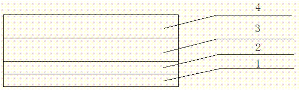
[0023] 1) Pretreatment of the original silicon wafer, the pretreatment includes processes such as texturing, diffusion and etching in the battery process;

[0024] 2) Use PECVD equipment to sequentially deposit multi-layer SiN whose refractive index decreases according to a certain rule on the surface of the polycrystalline silicon wafer after etching x layer, where the underlying SiN x layer, the refractive index is 2.25, and the film thickness is 10nm; the middle layer SiN x layer, the refractive index is 2.2, and the film thickness is 20nm; single-layer SiN x layer, the refractive index is 2.15, and the film thickness is 30nm;

[0025] 3) Use PECVD equipment to plate remaining SiO on the diffusion surface x Ny layer, the refractive index is 1.75, and the film thickness is 30nm;

[0026] 4) Print the back electrode, aluminum back field, positive grid line and positive electrode using the traditional battery printing process, and sinter them.

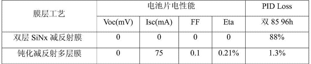
[0027] After testing, it i...

Embodiment 2

[0032] 1) Pretreatment of the original silicon wafer, the pretreatment includes processes such as texturing, diffusion and etching in the battery process;

[0033] 2) Use PECVD equipment to sequentially deposit multi-layer SiN whose refractive index decreases according to a certain rule on the surface of the polycrystalline silicon wafer after etching x layer, where the underlying SiN x layer, the refractive index is 2.25, and the film thickness is 5nm;

[0034] Intermediate SiN x layer, the refractive index is 2.20, and the film thickness is 15nm; double-layer SiN x layer, the first layer of SiN x The refractive index is 2.15, and the film thickness is 15nm; the second layer of SiN x The refractive index is 2.05, and the film thickness is 25nm;

[0035] 3) Use PECVD equipment to plate remaining SiO on the diffusion surface x N y layer, the refractive index is 1.8, and the film thickness is 35nm;

[0036] 4) Print the back electrode, aluminum back field, positive grid ...


PUM

PropertyMeasurementUnit
thicknessaaaaaaaaaa
thicknessaaaaaaaaaa
thicknessaaaaaaaaaa

Abstract

The invention relates to a high-efficiency polycrystalline multilayer passivation anti-reflection film structure with high PID resistance. The structure is characterized in that a bottom SiNx layer, an intermediate SiNx layer, a single-or multi-optical optimization SiNx layer, and a top optical optimization SiOxNy layer are successively arranged on a positive surface of a polycrystalline silicon sheet substrate from bottom to top, wherein the refractive indexes of the layers decrease gradually. The total film thickness is 70 to 135nm and the total refractive index is 1.95 to 2.20. According to the invention, on the basis of the traditional polycrystalline silicon battery process, only the membranous structure of the passivation anti-reflection film is changed and compatibility with the traditional polycrystalline silicon battery process is realized; production can be carried out only by modifying the common etching equipment and PECVD equipment slightly; no special requirement is provided; and the structure can be realized easily and is suitable for large-scale production. And the structure also can be applied to some advanced battery processes like a back passivation battery, an N type dual-face battery, and an MWT battery and the like.

Description

technical field [0001] The invention relates to the field of solar cell manufacturing, in particular to a high-efficiency polycrystalline multi-layer passivation anti-reflection film structure with high PID resistance. Background technique [0002] As environmental issues and energy issues have attracted more and more people's attention, solar cells, as a clean energy source, have entered a new stage in their research and development. The PID (potential induced degradation) effect refers to the phenomenon of leakage between the glass and the packaging material in the module under long-term high voltage, which causes the failure of the surface passivation anti-reflection film first, and then the failure of the PN junction, which finally reduces the performance of the module. P-type solar crystalline silicon modules with traditional technology have certain PID failure problems, so studying PID phenomena and developing PID-free solar cells is one of the goals of the R&D departm...

Claims


Application Information

Patent Timeline
Patent Type & Authority Patents(China)
IPC IPC(8): H01L31/0216
CPCH01L31/02168
Inventor 瞿辉徐春曹玉甲张一源
Owner JIANGSU SHUNFENG PHOTOVOLTAIC TECH CO LTD
Why Eureka
Try Eureka