GaN-based LED epitaxial structure preparation method for improving the crystal quality

A technology of crystal quality and epitaxial structure, applied in the direction of semiconductor devices, electrical components, circuits, etc., can solve the problems of high cost, affecting the crystal quality and performance of epitaxial wafers, etc., achieve good electrical yield, reduce atomization, reduce The effect of reverse leakage

Active Publication Date: 2015-07-01
LATTICE POWER (JIANGXI) CORP
View PDF2 Cites 1 Cited by
  • Summary
  • Abstract
  • Description
  • Claims
  • Application Information

AI Technical Summary

Problems solved by technology

[0004] However, this method of preparing LED epitaxial wafers is expensive, and some accessories need to be replaced every time a furnace of epitaxial wafers is grown, and there is a certain probability of fogging during the epitaxial growth process, which will affect the crystal quality and performance of the epitaxial wafers

Method used


Image

  • GaN-based LED epitaxial structure preparation method for improving the crystal quality
  • GaN-based LED epitaxial structure preparation method for improving the crystal quality

Examples


Embodiment 1

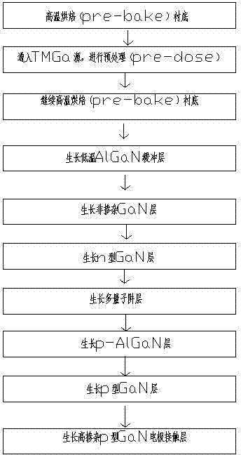
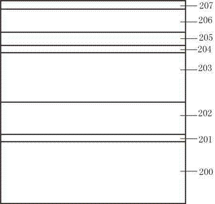
[0017] A method for preparing a GaN-based LED epitaxial structure with improved crystal quality, comprising the following steps:

[0018] Put the sapphire substrate with (0001) crystal orientation into the MOCVD reaction chamber, and then 2 Raise the temperature to 1180°C in the environment for high-temperature baking (pre-bake) the substrate, stabilize it for 400s, turn on the TMGa source, keep the TMGa flow rate at 25sccm for 30s, continue high-temperature baking (pre-dose) the substrate for 170s, and cool down to 550 ℃, grow a 30nm thick GaN buffer layer at 600mbar, raise the temperature to 1150℃ to grow a 2.5um thick non-doped GaN layer, and grow a 3um thick n-type GaN layer at 1150℃, in N 2 The multi-quantum well layer was grown for 12 cycles in the environment, the GaN barrier layer: the thickness is 13nm, the growth temperature is 850°C; the InGaN well layer: the thickness is 2nm, the growth temperature is 760°C, and the temperature is raised to 1000°C to grow 60nm thic...

Embodiment 2

[0020] A method for preparing a GaN-based LED epitaxial structure with improved crystal quality, comprising the following steps:

[0021] Put the sapphire substrate with (0001) crystal orientation into the reaction chamber, and then 2 The temperature was raised to 1200°C in the environment, and the substrate was pre-dose at high temperature, stabilized for 400s, and the TMGa source was connected, and the flow rate of TMGa was kept at 30sccm for 50s, and the substrate was pre-dose continued at high temperature for 150s, and the temperature was lowered to 550°C, grow a 10nm thick GaN buffer layer at 600mbar, raise the temperature to 1150°C to grow a 2.5um thick non-doped GaN layer, grow a 3um thick n-type GaN layer at 1150°C, and grow a 3um thick n-type GaN layer at 1150°C. 2 The multi-quantum well layer was grown for 12 cycles in the environment, the GaN barrier layer: the thickness is 13nm, the growth temperature is 850°C; the InGaN well layer: the thickness is 2nm, the growth...


PUM


Abstract

The invention provides a GaN-based LED epitaxial structure preparation method for improving the crystal quality. A TMGa source is introduced for a period of time during epitaxial growth of a GaN-based LED epitaxial film and pre-baking of a growth substrate at high temperature, and then the growth substrate continues to be pre-baked at high temperature. The substrate and the environment for epitaxial growth are improved without increasing the process complexity, the whole LED epitaxial layer has higher crystal quality, higher brightness and higher electrical yield, the atomization phenomenon is effectively reduced, and the production cost is lowered.

Description

technical field [0001] The invention relates to the technical field of LED production and preparation, in particular to a method for preparing a GaN-based LED epitaxial structure with improved crystal quality. Background technique [0002] Light Emitting Diode (LED, Light Emitting Diode) is a semiconductor solid-state light-emitting device, which uses a semiconductor PN junction as a light-emitting material, and can directly convert electricity into light. When a forward voltage is applied to both ends of the semiconductor PN junction, the minority carriers injected into the PN junction recombine with the majority carriers, releasing excess energy to cause photon emission, and the direct emission colors are red, orange, yellow, Green, blue, blue, purple light. Among them, the III-V compound semiconductors represented by gallium nitride (GaN) have the characteristics of wide band gap, high luminous efficiency, high electron saturation drift speed, and stable chemical propert...

Claims


Application Information

Patent Timeline
Patent Type & Authority Applications(China)
IPC IPC(8): H01L33/00H01L33/06H01L33/12
CPCH01L33/0066H01L33/0075
Inventor 向君余小明陈振
Owner LATTICE POWER (JIANGXI) CORP
Why Eureka
Try Eureka