Memristor and manufacturing method thereof

A technology of memristor and bottom electrode, which is applied in the field of non-volatile memory, can solve the problems of incomplete research on material system, unclear mechanism, and short research time of memristor, and achieve low cost, low operating voltage, The effect of simple preparation method

Inactive Publication Date: 2015-07-01
GENERAL RESEARCH INSTITUTE FOR NONFERROUS METALS BEIJNG
View PDF2 Cites 12 Cited by
  • Summary
  • Abstract
  • Description
  • Claims
  • Application Information

AI Technical Summary

Problems solved by technology

However, due to the short research time of memristors, the research on material systems is incomplete, and the mechanism is not clear enough, more research is needed to clarify its application prospects

Method used


Image

  • Memristor and manufacturing method thereof
  • Memristor and manufacturing method thereof
  • Memristor and manufacturing method thereof

Examples


Embodiment 1

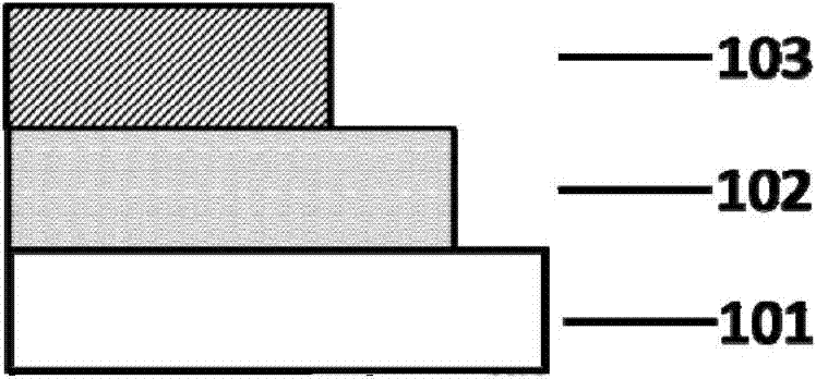
[0032] figure 1 It is a structural schematic diagram of the memristor of the vertical structure of the present invention, such as figure 1 As shown, the bottom of the structure is the substrate 101, the substrate 101 is used to support the structure of the entire memristor, and the substrate is used as the bottom electrode; a layer of single crystal cerium oxide film 102 is epitaxy on the substrate 101, Finally, a top electrode 103 is deposited on the cerium oxide film 102 .

[0033] The process flow of the preparation method of the memristor of the vertical structure of the present invention includes the following specific steps:

[0034] 1) Substrate cleaning, the substrate is Nb-doped SrTiO 3 , the substrate not only plays the role of making the whole device, but also serves as the bottom electrode.

[0035] 2) Laser Molecular Beam Epitaxy on Nb-doped SrTiO 3 (NSTO) Epitaxial CeO 2 Thin film, before deposition, the vacuum degree of the chamber is ~1×10 -7 Pa; during t...

Embodiment 2

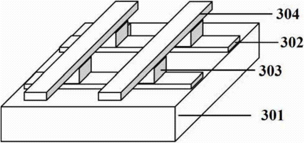
[0040] In this embodiment, the memristor is a cross-array structure, such as image 3 shown. The bottom end of the structure is the substrate 301, which is used as the bottom electrode in addition to supporting the entire memristor structure; the bottom electrode 302 (bit line) of the cross array is etched on the substrate 301; Epitaxial CeO on 302 2 Thin film 303; on CeO 2A top electrode 304 is deposited on top of the film. Such as Figure 4 , 5 Shown, its preparation process is specifically:

[0041] Step 401 (corresponding to 501): select heavily doped single crystal silicon (111) as a substrate, and clean it.

[0042] Step 402 (corresponding to 502): using reactive ion etching technology (reactive gas is CF 3 Br) directly forming a bottom electrode on the substrate;

[0043] Step 403 (corresponding to 503): using laser molecular beam epitaxy to epitaxially grow (111) crystal orientation CeO 2 The thin film is used as the material of the resistive switching functio...


PUM


Abstract

The invention provides a memristor and a manufacturing method thereof. The memristor comprises a top electrode and a bottom electrode; and a single crystal CeO2 storage medium layer. The manufacturing method comprises steps: (1) a substrate is cleaned; (2) etching technology is used for directly forming the bottom electrode on the substrate; (3) epitaxy technology is used for enabling a single crystal CeO2 thin film to be epitaxial on the bottom electrode to serve as resistance random function layer material; and (4) the top electrode is formed on the single crystal CeO2 thin film. The memristor of the invention is high in durability, low in operation voltage, good in data retention capability and free of activation. The memristor is simple in manufacturing method, low in cost and compatible with the traditional CMOS technology.

Description

technical field [0001] The invention relates to a memristor and a preparation method thereof, belonging to the technical field of non-volatile memory. Background technique [0002] Memory is a physical unit used to store data, programs, and files in electronic products. According to differences in data retention conditions, memories can be classified into volatile memories and nonvolatile memories. With volatile memory, stored data cannot be preserved after power is turned off, while non-volatile memory can. The microelectronics industry has long been looking for a non-volatile memory with high storage density, fast read and write, low cost, and low energy consumption. [0003] Cai Shaotang, a Chinese scientist at the University of California, Berkeley, first proposed the concept of memristor in 1971. Memristor, also known as memory resistance. When Professor Cai Shaotang studied the relationship between charge, current, voltage and magnetic flux, he deduced that besides...

Claims


Application Information

Patent Timeline
Patent Type & Authority Applications(China)
IPC IPC(8): H01L45/00
Inventor 赵鸿滨屠海令魏峰张艳杜军
Owner GENERAL RESEARCH INSTITUTE FOR NONFERROUS METALS BEIJNG
Why Eureka
Try Eureka