Phosphorus and boron liquid source one-shot perfect diffusion process

A liquid source and full diffusion technology, which is applied in semiconductor/solid-state device manufacturing, electrical components, circuits, etc., can solve the problems of poor anti-surge capability of devices, multiple reverse sources at the edge of silicon wafers, and uneven diffusion junction depth, etc., to achieve Small amount of reverse source, improved discharge resistance and reverse surge resistance, and the effect of reducing the concentration gradient

Active Publication Date: 2015-07-08
SUZHOU QILAN POWER ELECTRONICS
View PDF5 Cites 16 Cited by
  • Summary
  • Abstract
  • Description
  • Claims
  • Application Information

AI Technical Summary

Problems solved by technology

[0002] The manufacture of some devices in the semiconductor industry mostly uses the diffusion process to form a PN junction. At present, the commonly used diffusion process in the industry generally uses one-time full diffusion of phosphorus paper source and boron paper source or two-time diffusion of phosphorus and boron. These diffusion methods have problems. Defects to avoid: 1) The diffusion junction of paper source diffusion is not flat, there are many back sources on the edge of the silicon wafer, and the device’s anti-surge capability is poor; Sandblasting or chemical thinning to remove the anti-source amount, and then boron diffusion, the cost is high, and it is easy to cause debris

Method used


Image

  • Phosphorus and boron liquid source one-shot perfect diffusion process
  • Phosphorus and boron liquid source one-shot perfect diffusion process

Examples


Embodiment Construction

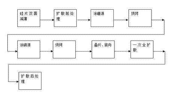
[0020] The primary total diffusion process of phosphorus and boron liquid sources according to the present invention will be further described in detail through specific examples below.

[0021] Such as figure 1 As shown, a phosphorus, boron liquid source once total diffusion process includes the following steps:

[0022] 1) Double-sided thinning of the silicon wafer: use nitric acid, hydrofluoric acid, and glacial acetic acid to etch the original silicon wafer on both sides according to the ratio of 3:1:1, and remove the surface damage layer;

[0023] 2) Cleaning before diffusion: chemically treat the surface of silicon wafers through acid, alkali and deionized water ultrasonic cleaning process;

[0024] 3) Coating boron source: place the cleaned silicon wafer on the rotator, drop the boron source on the center of the surface of the silicon wafer, start the rotator to rotate the silicon wafer, the rotation speed of the rotator is 3000-4000 rpm, The concentration of the Peng...


PUM


Abstract

The invention discloses a phosphorus and boron liquid source one-shot perfect diffusion process. The process is mainly implemented through the following steps that one surface of each silicon wafer with two thinned sides is rotated to be coated with a liquid boron source, baked and then rotated again to be coated with a liquid phosphorus source, lamination is conducted after baking, the silicon wafers are stacked on a silicon boat pairwise to be subjected to one-shot perfect diffusion in the mode that each phosphorus source surface is opposite to the corresponding phosphorus source surface and each boron source surface is opposite to the corresponding boron source surface. Diffused junction depth is even, and reverse breakdown voltage of a product can be stable and good in uniformity; the diffusion concentration gradient is reduced, PN junction field intensity can be effectively improved, discharging-resistant capacity of the product is improved, and the reverse surge capacity of the product can be effectively improved; meanwhile, the source return quantity of the edge of the silicon wafer is small, the number of intra defects is small, and product reliability is high. Processing cost is low, the process is simple, and production is easy.

Description

technical field [0001] The invention relates to a manufacturing process of a semiconductor device, in particular to a primary total diffusion process of phosphorus and boron liquid sources. Background technique [0002] The manufacture of some devices in the semiconductor industry mostly uses the diffusion process to form a PN junction. At present, the commonly used diffusion process in the industry generally uses one-time full diffusion of phosphorus paper source and boron paper source or two-time diffusion of phosphorus and boron. These diffusion methods have problems. Defects to avoid: 1) The diffusion junction of paper source diffusion is not flat, there are many back sources on the edge of the silicon wafer, and the device’s anti-surge capability is poor; Sandblasting or chemical thinning to remove the anti-source amount, followed by boron diffusion, is costly and prone to debris. Contents of the invention [0003] The technical problem to be solved by the present in...

Claims


Application Information

Patent Timeline
Patent Type & Authority Applications(China)
IPC IPC(8): H01L21/223
CPCH01L21/228
Inventor 丛培金范玉丰丛济洲
Owner SUZHOU QILAN POWER ELECTRONICS
Why Eureka
Try Eureka