The method of removing the residual gold of the lithography marking point of the LED chip

A technology of LED chip and lithography marking, which is applied to electrical components, electric solid devices, circuits, etc., can solve the problems that the metal of the LED chip should not be removed, and the residual gold of the lithography marking point of the LED chip, etc.

Active Publication Date: 2017-09-26
宁波安芯美半导体有限公司
View PDF4 Cites 0 Cited by
  • Summary
  • Abstract
  • Description
  • Claims
  • Application Information

AI Technical Summary

Problems solved by technology

[0006] Aiming at the deficiencies of the prior art, the present invention provides a method for solving the problem of residual gold in the photolithographic marking points of LED chips, which solves the problem that the residual metal on the existing LED chips is not suitable for removal

Method used


Image

  • The method of removing the residual gold of the lithography marking point of the LED chip
  • The method of removing the residual gold of the lithography marking point of the LED chip
  • The method of removing the residual gold of the lithography marking point of the LED chip

Examples


Embodiment 1

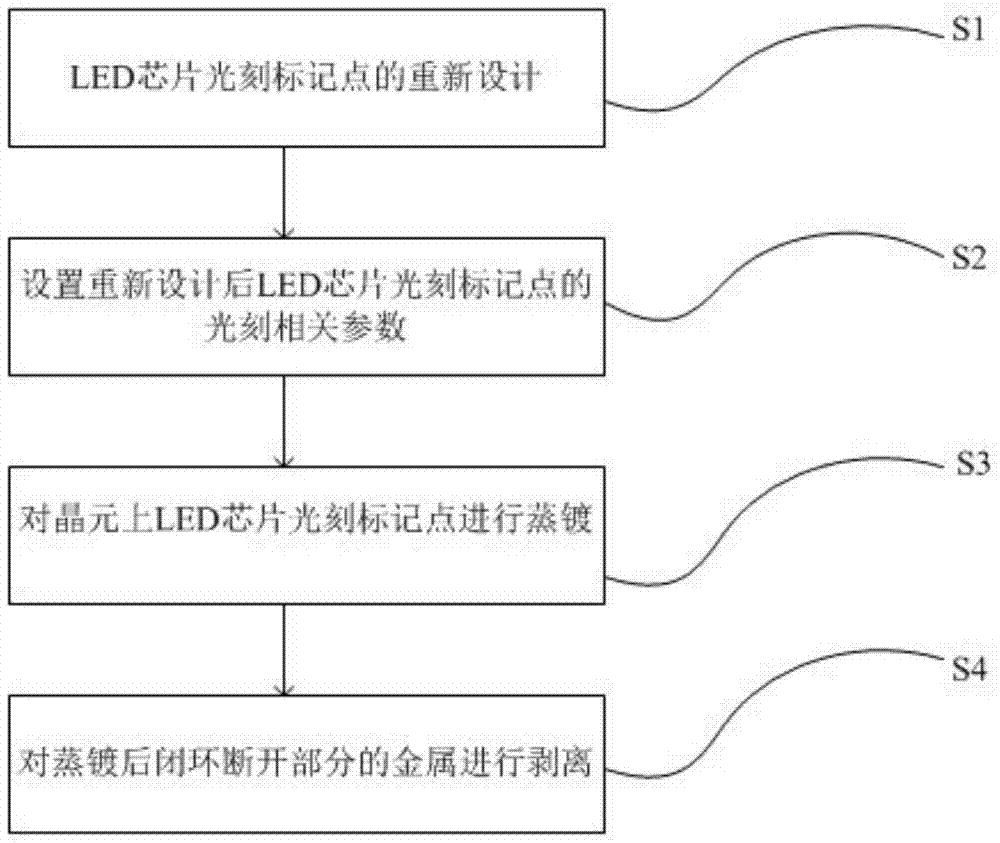
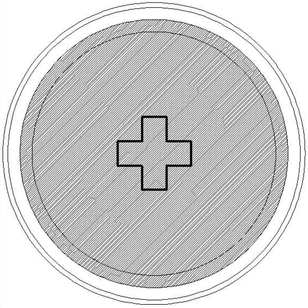
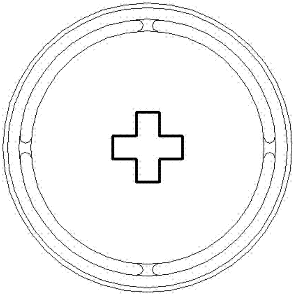
[0045] combine figure 2 with image 3 Describe the specific workflow, a method for removing residual gold at photolithographic marking points of LED chips, including redesigning the photolithographic marking points of LED chips, setting the width of the broken part of the ring to 15 μm, and fixing the opening direction of the broken part of the ring. The angle range is 45°, the fillet radius of the broken part of the ring is 7 μm, and the broken part of the ring adopts the method of large inside and small outside; set the lithography-related parameters of the lithography marking points of the LED chip after the redesign, and evenly The gel soft-baking temperature is 113°C, the exposure dose is 60mJ, the PEB temperature is 106°C, and the development time is 100s, then stand still. According to the parameters, the temperature of the photolithographic marking point of the LED chip is set for vapor deposition, and then the photolithographic marking point of the LED chip on the w...

Embodiment 2

[0047] combine Figure 4 with Figure 5 Describe the specific workflow, a method for removing residual gold from photolithographic marking points of LED chips, including redesigning the photolithographic marking points of LED chips, setting the width of the disconnected part of the square ring to 15 μm, and fixing the opening direction of the disconnected part of the square ring. The angle range is 45°, the fillet radius of the disconnected part of the square ring is 7 μm, and the disconnected part of the square ring adopts the method of large inside and small outside; set the lithography-related parameters of the lithography marking points of the LED chip after the redesign, uniform The gel soft-baking temperature is 113°C, the exposure dose is 60mJ, the PEB temperature is 106°C, the development time is 100s, and then stand still. According to the parameters, the temperature of the photolithographic marking point of the LED chip is set for vapor deposition, and then the phot...


PUM


Abstract

The invention provides a method for removing residual gold at photolithographic marking points of LED chips, and relates to the technical field of LED chip production. The method includes: redesigning the lithography marking points of the LED chip; setting the lithography-related parameters of the lithography marking points of the LED chip after the redesign; setting the lithography marking points of the LED chip according to the parameters for evaporation temperature, and then vapor-deposit the photolithographic mark points of the LED chip on the wafer; after the vapor deposition of the photolithographic mark points of the LED chip is completed, the metal stripping process conditions are set, and the metal of the closed-loop disconnected part is stripped; Glue removal is performed on the closed-loop disconnected part on the photolithographic marking point of the LED chip after the metal is peeled off. The invention solves the problem that photolithography cannot be carried out after gold plating of the LED chip due to residual metal, thereby reducing the rework rate of preparation, ensuring product consistency, removing unstable factors, and improving product yield.

Description

technical field [0001] The invention relates to the technical field of LED chip production, in particular to a method for removing residual gold at photoetched ring marking points of LED chips. Background technique [0002] Evaporation is a process of vapor-depositing metal on the surface of the film substrate under vacuum conditions to form a composite film. [0003] In the existing LED chip metal evaporation and photolithography, closed-loop and in-loop graphics are generally used to achieve the purpose of overlaying. There are generally many layers of complex graphics on semiconductor and LED chips, and alignment between layers is required. The main function of marking points is to align between multiple exposures. Generally, a pattern is made on the first layer. Graphics (the first layer does not need to be aligned), use the graphics on each subsequent layer of photolithography (usually a closed loop) to align / register with the graphics on the first layer to achieve ali...

Claims


Application Information

Patent Timeline
Patent Type & Authority Patents(China)
IPC IPC(8): H01L23/544
Inventor 吴永军
Owner 宁波安芯美半导体有限公司
Why Eureka
Try Eureka