Method for analyzing failures due to defects of ONO (silicon oxide-silicon nitride-silicon oxide) thin films of Flash products

A failure analysis and thin film defect technology, which is applied in the direction of electrical components, circuits, semiconductor/solid-state device testing/measurement, etc., can solve problems such as indistinguishable, ONO thin film interference, etc., and achieve the effect of improving yield and reliability, and improving efficiency

Active Publication Date: 2015-07-22
SHANGHAI HUALI MICROELECTRONICS CORP
View PDF8 Cites 9 Cited by
  • Summary
  • Abstract
  • Description
  • Claims
  • Application Information

AI Technical Summary

Problems solved by technology

However, when using TEM to observe the sample, since it is imaged through the contrast of scattering, absorption, interference and diffraction that occurs when the high-energy electron beam penetrates the sample, the defects of the ONO film are often very small, and its The upper and lower sides are covered by the polysilicon layer, so that the defects of the ONO film are easily disturbed by the polysilicon layer and cannot be distinguished during imaging.

Method used


Image

  • Method for analyzing failures due to defects of ONO (silicon oxide-silicon nitride-silicon oxide) thin films of Flash products
  • Method for analyzing failures due to defects of ONO (silicon oxide-silicon nitride-silicon oxide) thin films of Flash products
  • Method for analyzing failures due to defects of ONO (silicon oxide-silicon nitride-silicon oxide) thin films of Flash products

Examples


Embodiment Construction

[0026] The specific embodiment of the present invention will be further described in detail below in conjunction with the accompanying drawings.

[0027] It should be noted that, in the following specific embodiments, when describing the embodiments of the present invention in detail, in order to clearly show the structure of the present invention for the convenience of description, the structures in the drawings are not drawn according to the general scale, and are drawn Partial magnification, deformation and simplification are included, therefore, it should be avoided to be interpreted as a limitation of the present invention.

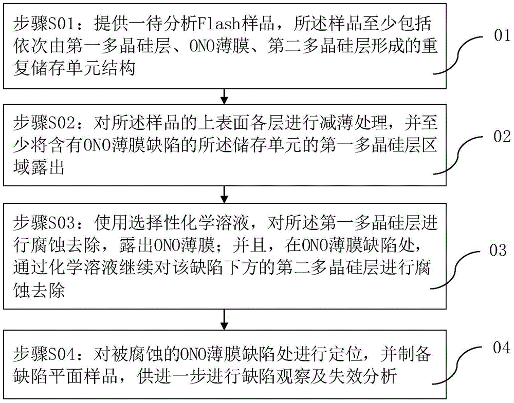
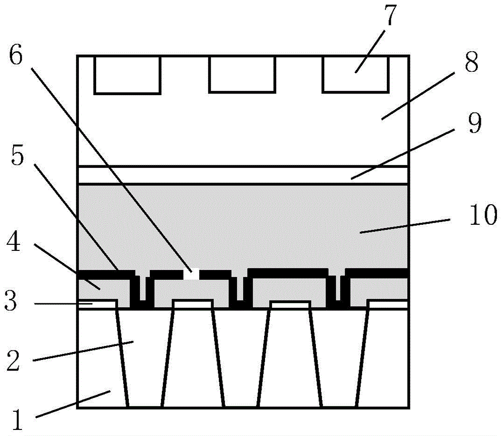
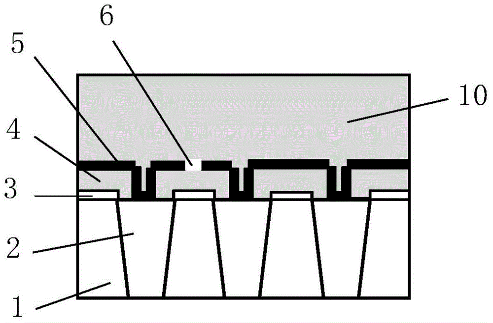
[0028] In the following specific embodiments of the present invention, please refer to figure 1 , figure 1 It is a flow chart of the failure analysis method for the ONO film defect of a Flash product of the present invention; meanwhile, please refer to Figure 2 to Figure 5 as well as Figure 6 ~ Figure 9 ,in, Figure 2 to Figure 5 is used in an ...


PUM


Abstract

The invention discloses a method for analyzing failures due to defects of ONO (silicon oxide-silicon nitride-silicon oxide) thin films of Flash products. The method includes thinning various layers of the upper surfaces of to-be-analyzed Flash samples and exposing first polycrystalline silicon layer regions of storage units; corroding and removing first polycrystalline silicon layers by the aid of selective chemical solution and exposing the ONO thin films; corroding and removing second polycrystalline silicon layers below the defects of the ONO thin films by the aid of the chemical solution and positioning the corroded defects of the ONO thin films; manufacturing planar samples of the defects for further observing the defects and analyzing the failures. The first polycrystalline silicon layer regions of the storage units contain the defects of the ONO thin films. The method has the advantages that the defects of the ONO thin films of the Flash products can be conveniently, accurately and finely analyzed, accordingly, the failure analysis efficiency can be greatly improved, and the method can assist in quickly increasing the yield of the Flash products and quickly improving the reliability of the Flash products.

Description

technical field [0001] The invention relates to the technical field of semiconductor integrated circuit manufacturing, and more specifically, to a failure analysis method for ONO film defects of Flash products. Background technique [0002] During the processing of semiconductor devices, some defects often occur, and these defects will cause the final formed semiconductor device or even the entire chip to fail. In order to detect and solve process problems in the production process of integrated circuits as soon as possible, once a test failure is found, a failure analysis will be carried out immediately to confirm the process steps that caused the problem, so that the production line can make timely improvements. Therefore, the failure analysis of semiconductor chips (devices) is an important task to confirm various failure causes and improve product quality and reliability. [0003] Flash (flash memory) product is the most popular storage product at present, it has the ch...

Claims


Application Information

Patent Timeline
Patent Type & Authority Applications(China)
IPC IPC(8): H01L21/66
CPCH01L22/30
Inventor 陈强
Owner SHANGHAI HUALI MICROELECTRONICS CORP
Why Eureka
Try Eureka