X-ray flat panel detector
A flat-panel detector, X-ray technology, applied in the field of flat-panel detection, can solve the problems of reducing the detection efficiency and sensitivity of the X-ray detector, reducing the output efficiency, etc., and achieve the effect of improving the quantum detection efficiency and sensitivity
- Summary
- Abstract
- Description
- Claims
- Application Information
AI Technical Summary
Problems solved by technology
Method used
Image
Examples
Embodiment 1
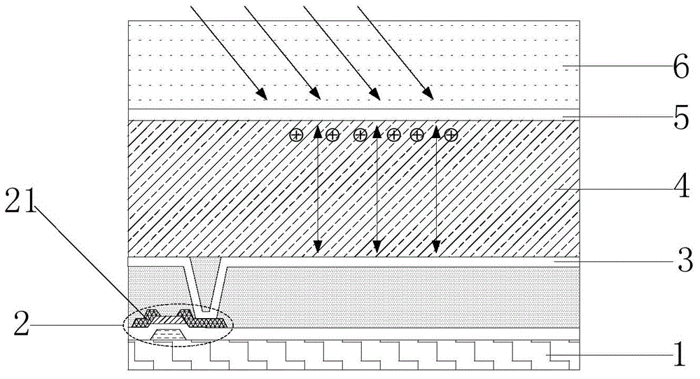
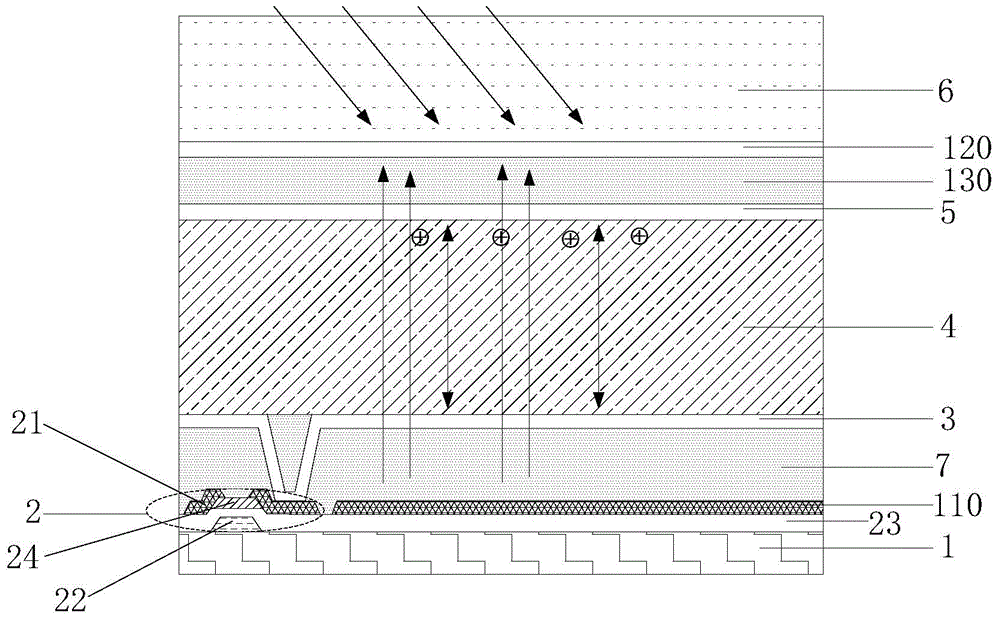
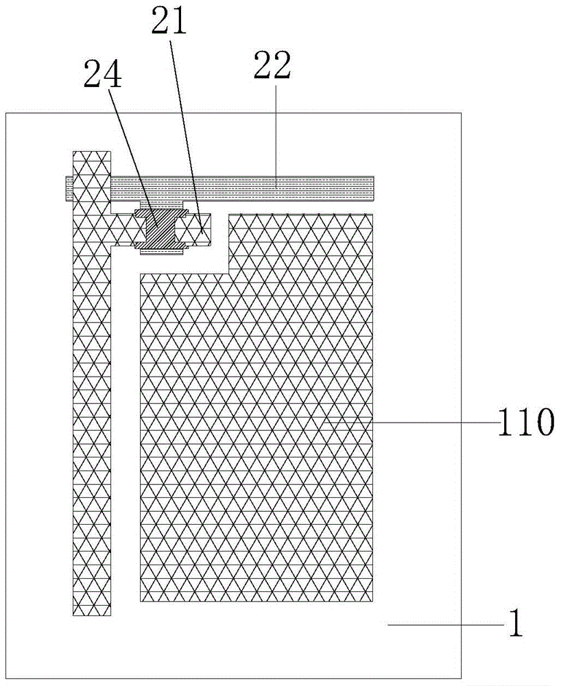
[0039] figure 2 It is a schematic cross-sectional structure diagram of the X-ray flat panel detector according to the first embodiment of the present invention. Such as figure 2As shown, in the first embodiment, the X-ray flat panel detector includes a substrate 1 with a general structure, a thin film transistor 2 disposed on the substrate, a pixel electrode layer 3, a photodiode 4, a transparent electrode layer 5 and In addition to the X-ray conversion layer 6, it also includes a positive electrode layer 110 and a negative electrode layer 120, wherein the negative electrode layer 120 is made of a light-transmitting material, and is arranged between the transparent electrode layer 5 and the X-ray conversion layer 6, the transparent electrode layer 5 and the X-ray conversion layer 6 A light-transmitting insulating layer 130 is also arranged between the negative electrode layers 120, and the insulation between the transparent electrode layer 5 and the X-ray conversion layer 6...
Embodiment 2
[0051] Figure 4 It is a schematic cross-sectional structure diagram of the X-ray flat panel detector according to the second embodiment of the present invention. Such as Figure 4 As shown, in the second embodiment, the X-ray flat panel detector includes a substrate 1 with a general structure, a thin film transistor 2 disposed on the substrate 1, a pixel electrode layer 3, a photodiode 4, and a transparent electrode layer 5 In addition to the X-ray conversion layer 6, it also includes a positive electrode layer 210 and a negative electrode layer 220, and the negative electrode layer 220 is made of a transparent material. Specifically, the transparent electrode layer 5 and the negative electrode layer 220 are arranged in the same layer and material and are insulated from each other, and the positive electrode layer 210 and the gate 22 of the thin film transistor 2 are arranged in the same layer and made of the same material.
[0052] Preferably, the electrodes of the transpa...
Embodiment 3
[0067] Figure 7 It is a schematic cross-sectional structure diagram of the X-ray flat panel detector according to the third embodiment of the present invention. Such as Figure 7 As shown, in the third embodiment, in the third embodiment, the X-ray flat panel detector includes a substrate 1 with a general structure, a thin film transistor 2 disposed on the substrate 1, a pixel electrode layer 3, a photoelectric In addition to the diode 4, the transparent electrode layer 5 and the X-ray conversion layer 6, it also includes a positive electrode layer 310 and a negative electrode layer 320, and the negative electrode layer 320 is made of a transparent material. Specifically, the transparent electrode layer 5 and the negative electrode layer 320 are in the same layer and material and are insulated from each other, and the positive electrode layer 310 and the pixel electrode layer 3 are in the same layer and material and are insulated from each other.
[0068] In addition, prefe...
PUM
 Abstract
Description
Claims
Application Information


