CMOS transistor and forming method thereof

A transistor and semiconductor technology, applied in the manufacture of transistors, semiconductor devices, semiconductor/solid-state devices, etc., can solve problems such as poor performance of CMOS transistors

Active Publication Date: 2015-07-29
SEMICON MFG INT (SHANGHAI) CORP +1
View PDF7 Cites 19 Cited by
  • Summary
  • Abstract
  • Description
  • Claims
  • Application Information

AI Technical Summary

Problems solved by technology

[0004] The existing CMOS transistors formed by the above-mentioned gate-last process have poor performance

Method used


Image

  • CMOS transistor and forming method thereof
  • CMOS transistor and forming method thereof
  • CMOS transistor and forming method thereof

Examples


Embodiment Construction

[0031] As mentioned in the background art, the performance of the CMOS transistors formed in the prior art is relatively poor and needs to be further improved.

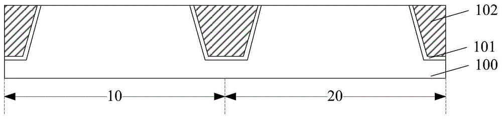
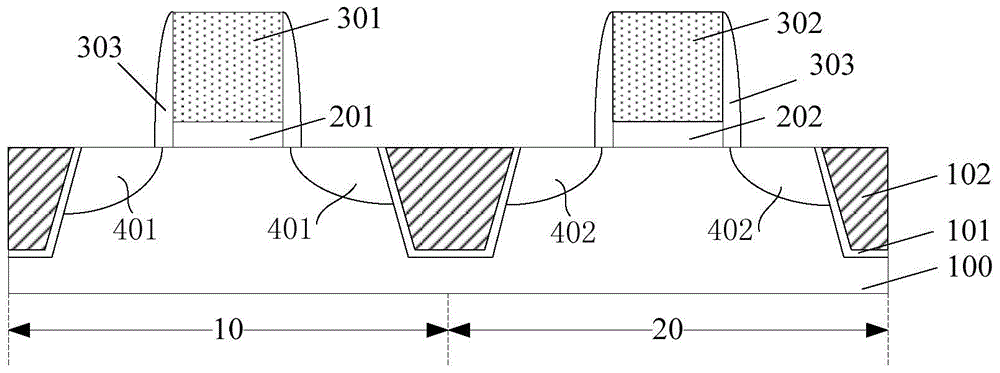
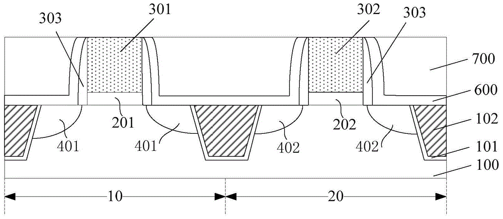
[0032] It is found through research that the metal gate of the CMOS transistor is generally made of metal materials such as Al and Cu, and the metal atoms in the metal gate will diffuse into the work function layer, affecting the work function of the CMOS transistor; and, because The size of the CMOS transistor is small, the thickness of the work function layer is low, and the metal atoms will also diffuse into the high-K gate dielectric layer through the work function layer, affecting the dielectric constant of the high-K gate dielectric layer, and easily A gate leakage current is formed, thereby affecting the performance of the CMOS transistor. The diffusion of metal atoms can be blocked by forming a barrier layer on the surface of the gate dielectric layer, but due to the small size of the groove, only a barrier la...


PUM


Abstract

Disclosed are a CMOS transistor and a forming method thereof. The method includes the following steps: providing a semiconductor substrate which includes an NMOS area and a PMOS area, wherein a dielectric layer is formed on the surface of the semiconductor substrate, a first grove is arranged in the dielectric layer on the NMOS area, a second groove is arranged in the dielectric layer on the PMOS area and both of the first groove and the second groove are exposed out of the part of the semiconductor substrate; forming a gate dielectric layer on the inner surfaces of the first groove and the second groove and a coverage layer on the surface of the gate dielectric layer, wherein the coverage layer is doped with non-proliferation ions; forming a barrier layer on the surface of the coverage layer; forming a first work function layer on the surface of the barrier layer in the second groove; forming a second work function layer on the surface of the barrier layer in the first groove and on the surface of the first work function layer in the second groove; and forming a grid electrode layer, which fills fully the first groove and the second groove, on the surface of the second work function layer.

Description

technical field [0001] The invention relates to the technical field of semiconductors, in particular to a CMOS transistor and a forming method thereof. Background technique [0002] With the continuous improvement of the integration level of semiconductor devices and the reduction of technology nodes, the traditional gate dielectric layer continues to become thinner, and the leakage of transistors increases accordingly, causing problems such as waste of power consumption of semiconductor devices. In order to solve the above problems, the prior art provides a solution of replacing the polysilicon gate with a metal gate. Among them, the "gate last" process is a main process for forming high-K metal gate transistors. [0003] The existing method for forming a high-K metal gate transistor using a gate-last process includes: providing a semiconductor substrate on which a dummy gate structure is formed and located on the semiconductor substrate and covering the dummy gate structu...

Claims


Application Information

Patent Timeline
Patent Type & Authority Applications(China)
IPC IPC(8): H01L27/092H01L29/06H01L21/8238
Inventor 谢欣云
Owner SEMICON MFG INT (SHANGHAI) CORP
Why Eureka
Try Eureka