Tunneling field effect transistor and preparation method

A tunneling field effect and transistor technology, which is applied in semiconductor/solid-state device manufacturing, semiconductor devices, electrical components, etc., can solve the problems of high subthreshold slope of devices and unfavorable application of TFET devices, etc., and achieve large-band tunneling current increase The effect of reducing the minimum subthreshold slope and reducing the production cost

Active Publication Date: 2015-07-29
PEKING UNIV
View PDF4 Cites 8 Cited by
  • Summary
  • Abstract
  • Description
  • Claims
  • Application Information

AI Technical Summary

Problems solved by technology

[0003] However, unlike traditional MOSFETs, the subthreshold slope in the subthreshold region of the TFET transfer curve changes and gradually increases with the increase of the gate voltage, which leads to a TFET transfer characteristic l...

Method used


Image

  • Tunneling field effect transistor and preparation method
  • Tunneling field effect transistor and preparation method
  • Tunneling field effect transistor and preparation method

Examples


Embodiment Construction

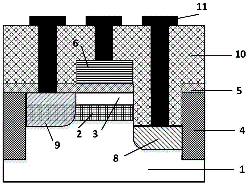
[0040] The implementation method of the heterostructure tunneling field effect transistor in the vertical channel direction of the present invention will be further described through specific embodiments below in conjunction with the accompanying drawings.

[0041] The specific implementation steps are as Figure 2-Figure 6 Shown: (This example takes N-type devices as an example, and P-type devices can be deduced by analogy)

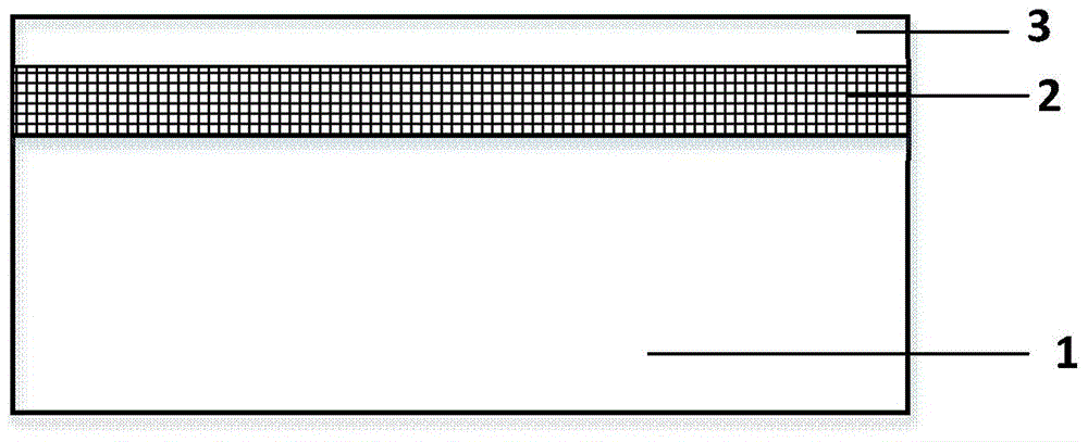
[0042] 1. The substrate doping concentration is lightly doped (about 1E13cm -3 -1E15cm -3 ), an InAs intermediate layer 2 is epitaxially grown on a GaAs substrate 1 with a crystal orientation of and lightly doped in situ (about 1E13cm -3 -1E15cm -3 ), with a thickness of about 15nm; then epitaxially grow a layer of GaAs upper layer 3 material and perform in-situ light doping (about 1E13cm -3 -1E15cm -3 ), the thickness is about 6nm; if figure 1 shown.

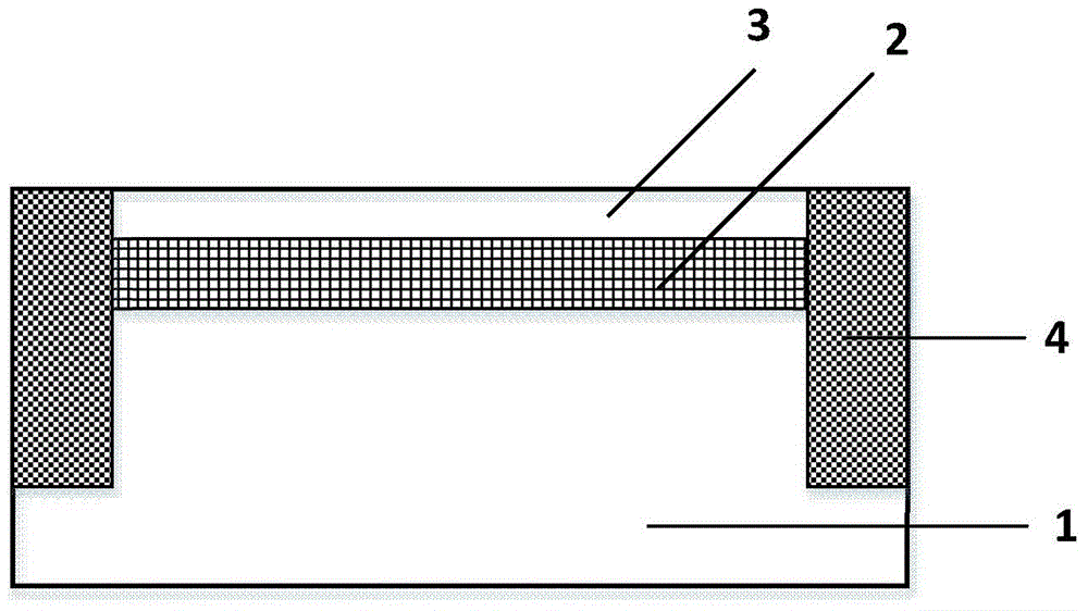
[0043] 2. Deposit a layer of silicon dioxide with a thickness of about 10nm, and deposit a lay...


PUM

PropertyMeasurementUnit
Thicknessaaaaaaaaaa
Thicknessaaaaaaaaaa

Abstract

The invention discloses a tunneling field effect transistor and a preparation method, and belongs to the field of a field effect transistor logic device of a CMOS (Complementary Metal Oxide Semiconductor) ultra-large scale integrated circuit (ULSI). A tunneling source region and a channel region of the tunneling field effect transistor are of heterogeneous structures in the vertical direction of the device; the upper layer is made of a semiconductor material with larger forbidden bandwidth; the middle layer is made of a semiconductor material with smaller forbidden bandwidth; the lower layer is a semiconductor substrate with the larger forbidden bandwidth. Compared with the prior art, the transistor and the method have the advantages that the degradation phenomenon of sub-threshold slope in device transfer characteristic can be effectively inhibited, meanwhile the average sub-threshold slope of the tunneling field effect transistor is obviously reduced, and steep minimum sub-threshold slope is kept.

Description

technical field [0001] The invention belongs to the field of CMOS ultra large scale integrated circuit (ULSI) field effect transistor logic devices, and in particular relates to a vertical channel direction heterogeneous structure tunneling field effect transistor and a preparation method thereof. Background technique [0002] Since the birth of integrated circuits, microelectronics integration technology has been developing continuously in accordance with "Moore's Law", and the size of semiconductor devices has been continuously reduced. As semiconductor devices enter the deep submicron range, traditional MOSFET devices are limited by the conduction mechanism of self-diffusion drift, and the subthreshold slope is limited by the thermoelectric potential kT / q, which cannot be reduced synchronously with the reduction of device size. As a result, the reduction of leakage current of MOSFET devices cannot meet the requirements of device size reduction, the energy consumption of t...

Claims


Application Information

Patent Timeline
IPC IPC(8): H01L29/78H01L29/08H01L21/336
CPCH01L29/0847H01L29/1033H01L29/66477H01L29/78
Inventor 黄如吴春蕾黄芊芊王佳鑫王阳元
Owner PEKING UNIV
Why Eureka
Try Eureka