

Electrostatic protection circuit
An electrostatic protection and circuit technology, applied in the direction of emergency protection circuit devices, circuits, circuit devices, etc., can solve the problems of unintentional MOS transistors, internal circuit operation failures, and insufficient startup of power supply voltage.
- Summary
- Abstract
- Description
- Claims
- Application Information
AI Technical Summary
Problems solved by technology
Method used
Image

Examples
no. 1 example
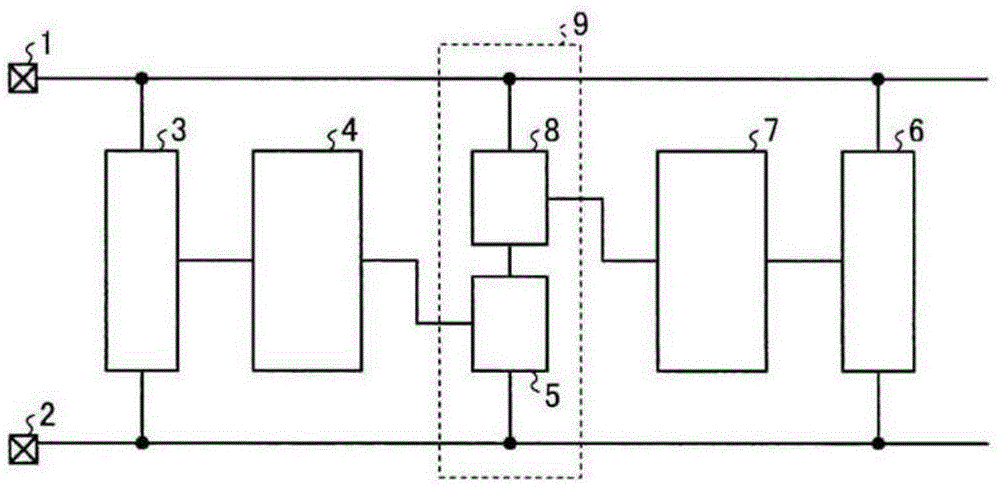
[0029] figure 1 is a schematic diagram showing the electrostatic protection circuit according to the first embodiment. The electrostatic protection circuit according to the embodiment includes a first trigger circuit 3 connected between the first power terminal 1 and the second power terminal 2 . The trigger signal of the first trigger circuit 3 is supplied to the first buffer circuit 4 . The first buffer circuit 4 amplifies the trigger signal from the first trigger circuit 3 and supplies the amplified trigger signal to the first switch circuit 5 . The conduction of the first switch circuit 5 is controlled by a driving signal from the first buffer circuit 4 .
[0030] The second trigger circuit 6 is connected in parallel with the first trigger circuit 3 between the first power supply terminal 1 and the second power supply terminal 2 . The trigger signal of the second trigger circuit 6 is supplied to the second buffer circuit 7 . The second buffer circuit 7 amplifies the tr...
no. 2 example
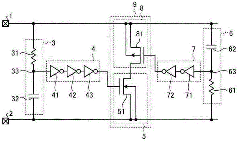
[0036] figure 2is a schematic diagram showing an electrostatic protection circuit according to the second embodiment. The same reference numerals and symbols are attached to the constituent elements corresponding to those of the above-described embodiment. In this embodiment, the first trigger circuit 3 includes a series circuit of a resistor 31 and a capacitor 32 . A common node 33 of the resistor 31 and the capacitor 32 is connected to the first buffer circuit 4 . The first buffer circuit 4 includes three stages of inverters 41 , 42 , 43 connected in series. For example, each of the inverters 41, 42, 43 is configured with a CMOS inverter. The first buffer circuit 4 amplifies the trigger signal from the first trigger circuit 3 and supplies the drive signal to the first switch circuit 5 . The first switch circuit 5 includes an NMOS transistor 51 . The drive signal from the first buffer circuit 4 is supplied to the gate electrode of the NMOS transistor 51 . The source el...
no. 3 example
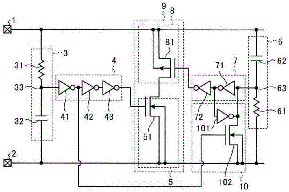
[0046] image 3 is a schematic diagram showing an electrostatic protection circuit according to the third embodiment. The same reference numerals and signs are attached to the constituent elements corresponding to those of the above-described embodiment, and their descriptions are omitted. The present embodiment includes a holding unit 10 that holds the level of the input signal of the second buffer circuit 7 for a predetermined time. The holding unit 10 includes an inverter 101 connected in antiparallel to the inverter 71 of the second buffer circuit 7 . For example, the inverter 101 is configured with a CMOS inverter. A feedback circuit is constituted in which, if the potential at the common node 63 becomes high level, an output signal of low level is supplied from the inverter 71 to the inverter circuit 101, and a signal of high level is supplied from the inverter circuit 101 to the inverter circuit 101. The phaser 101 is supplied to the inverter 71 . The input signal l...
PUM
 Abstract
Description
Claims
Application Information