Semi-automatic eutectic soldering method of GaAs microwave power amplifier chip and product

A technology for eutectic welding and power amplifier chips, which is used in welding equipment, semiconductor devices, semiconductor/solid-state device manufacturing, etc. Uniformity and other problems, to achieve the effect of reducing welding void rate, improving welding quality and low cost

Active Publication Date: 2016-09-28
HUBEI SANJIANG SPACE XIANFENG ELECTRONICS&INFORMATION CO LTD
View PDF8 Cites 16 Cited by
  • Summary
  • Abstract
  • Description
  • Claims
  • Application Information

AI Technical Summary

Problems solved by technology

[0004] When this process method is used for eutectic soldering, the solder can be fully melted. However, in this solution, the solder overflows around the chip unevenly, and the void area is relatively large, generally about 20%. In some products that require high frequency bands and low grounding resistance , the void ratio cannot meet the requirements of use
In addition, due to poor fluidity of gold-tin solder and easy pollution and oxidation of chips at high temperatures, semi-automatic eutectic soldering of chips is prone to false soldering, and the success rate of one-time soldering is low

Method used


Image

  • Semi-automatic eutectic soldering method of GaAs microwave power amplifier chip and product

Examples


Embodiment Construction

[0034] In order to make the object, technical solution and advantages of the present invention more clear, the present invention will be further described in detail below in conjunction with the examples. It should be understood that the specific embodiments described here are only used to explain the present invention, not to limit the present invention. In addition, the technical features involved in the various embodiments of the present invention described below can be combined with each other as long as they do not constitute a conflict with each other.

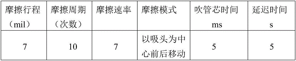
[0035] According to the semi-automatic eutectic welding process method of GaAS microwave power amplifier chip according to one embodiment of the present invention, it adds cleaning and preheating the chip on the basis of the existing eutectic welding method, and carries out tinning to the chip and the carrier The process steps and process parameters are optimized, so that chips with less void rate, less virtual soldering...


PUM


Abstract

The invention discloses a semi-automatic eutectic soldering method of a GaAs microwave power amplifier chip. The method comprises the following steps: (1) a carrier, a solder and a bare chip are cleaned; (2) the power amplifier bare chip is plated with tin; (3) the carrier is plated with tin; and (4) the eutectic soldering is performed, that is, the tin-plated bare chip is preheated; an eutectic heating soldering table provided with the tin-plated carrier is heated; meanwhile, nitrogen is opened for protection; the bare chip is absorbed; an auxiliary heating table is stopped heating; when the eutectic heating soldering table is heated above a certain temperature, the bare chip is eutectically rubbed on the carrier after accurate alignment; and the carrier is cleaned after natural cooling in air. The invention further discloses the GaAs microwave power amplifier chip prepared by the method. The method can prepare the chip with lower voidage, less pseudo soldering and excellent performances through controlling such process details as cleaning, preheating and tin plating in specific process and optimizing process parameters therein, and largely increases the welding success rate.

Description

technical field [0001] The invention belongs to the technical field of GaAs microwave power amplifier chips, and in particular relates to a GaAs microwave power amplifier chip eutectic welding method and a prepared product thereof. Background technique [0002] The connection between the GaAs microwave power amplifier chip and the substrate (substrate) requires good microwave grounding capability (low ohmic contact) and good heat dissipation capability. Gold-tin alloy solder is usually used for eutectic welding in the industry. [0003] At present, a typical solution in the prior art is to use a semi-automatic eutectic chip mounter for eutectic welding of GaAs microwave power amplifier chips. The specific process of this welding process includes: Put the carrier on top, release nitrogen to protect the working surface of the carrier, when heated to 300°C±10°C, absorb the gold-tin solder sheet and place it on the carrier to be soldered, and manually control the vacuum suction ...

Claims


Application Information

Patent Timeline
Patent Type & Authority Applications(China)
IPC IPC(8): B23K1/005B23K1/20H01L21/48H01L21/58
CPCB23K1/005B23K1/20B23K1/206B23K2101/36H01L21/48H01L24/83H01L2224/83009H01L2224/8301H01L2224/83022H01L2224/83024H01L2224/83805
Inventor 刘东洋秦钢李珊
Owner HUBEI SANJIANG SPACE XIANFENG ELECTRONICS&INFORMATION CO LTD
Why Eureka
Try Eureka