


Quick Research
Generate reliable direction feasibility study reports for your R&D in just a few steps.

Technical Q&A
Discover and master advanced knowledge NOW. Basics, ideas, possibilities, all at once.

Find Solutions
As an expert in R&D theories, this can generate solutions to your technical problems instantly.

Evaluate Feasibility
Analyze your overall solution with one click, know your potential R&D risks in advance.

Monitor Landscape
Get weekly tech updates, stay abreast of the latest tech innovations and key insights.
Electrostatic protection circuit
An electrostatic protection and circuit technology, applied in the direction of circuits, electrical components, electric solid devices, etc., can solve the problems of protection ability influence, lack of IOpad current path, etc.
- Summary
- Abstract
- Description
- Claims
- Application Information
AI Technical Summary
Problems solved by technology
Method used
Image

Examples
Embodiment 1
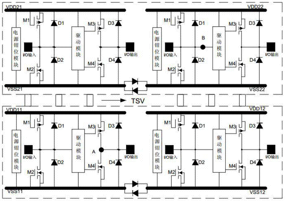
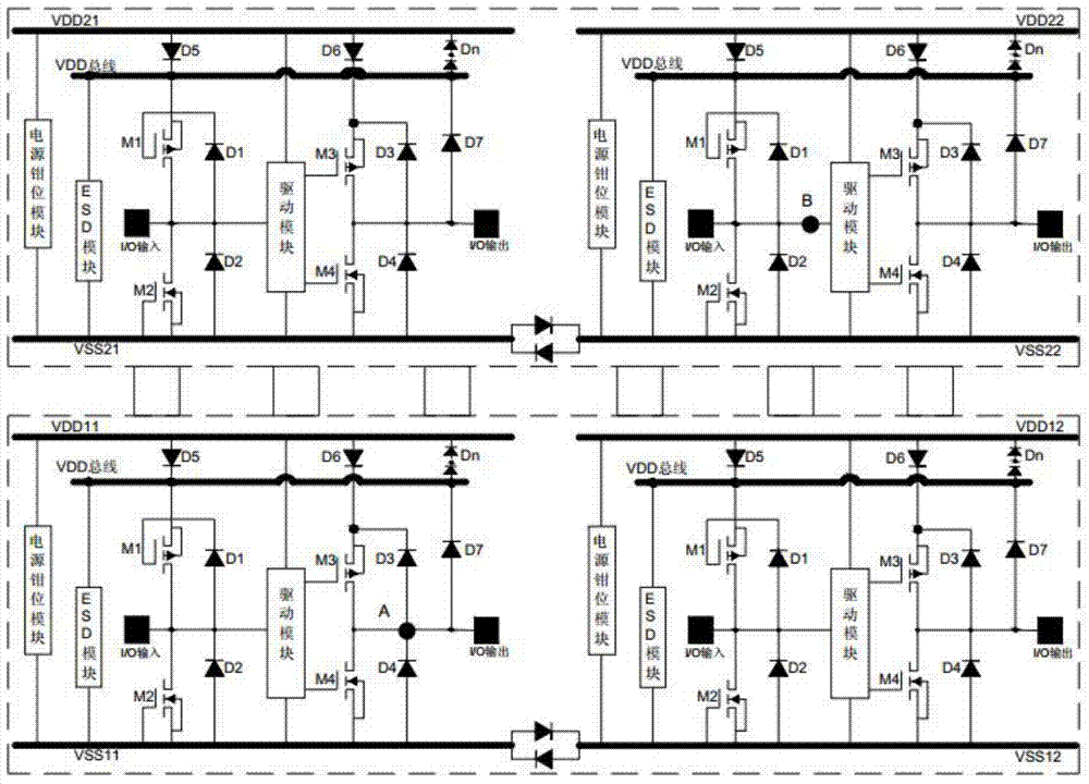
[0042] Specifically, such as image 3As shown, an electrostatic protection circuit mainly includes various components, specifically transistor M1, transistor M2, transistor M3, transistor M4, diode D5, diode D6, power supply voltage VDD, power supply voltage VSS, VDD bus (Dummy VDD), I / O input terminal (Innput Pad), I / O output terminal (Output Pad), power clamp module (Power Clamp), ESD module (Local ESD Clamp) and drive module (including logic circuit unit (Logic Circuits ) and a pre-driver unit (Pre-driver)), and the drive module has an input port (that is, a port connected to the I / O input terminal), a first drive port (that is, a port connected to the gate of the transistor M3), a second A driving port (that is, a port connected to the gate of transistor M4 ) and two return ports (ports connected to power supply voltages VDD and VSS ). The driving module realizes the on-off control of the transistor M3 or the transistor M4 through the first driving port and the second dri...
Embodiment 2
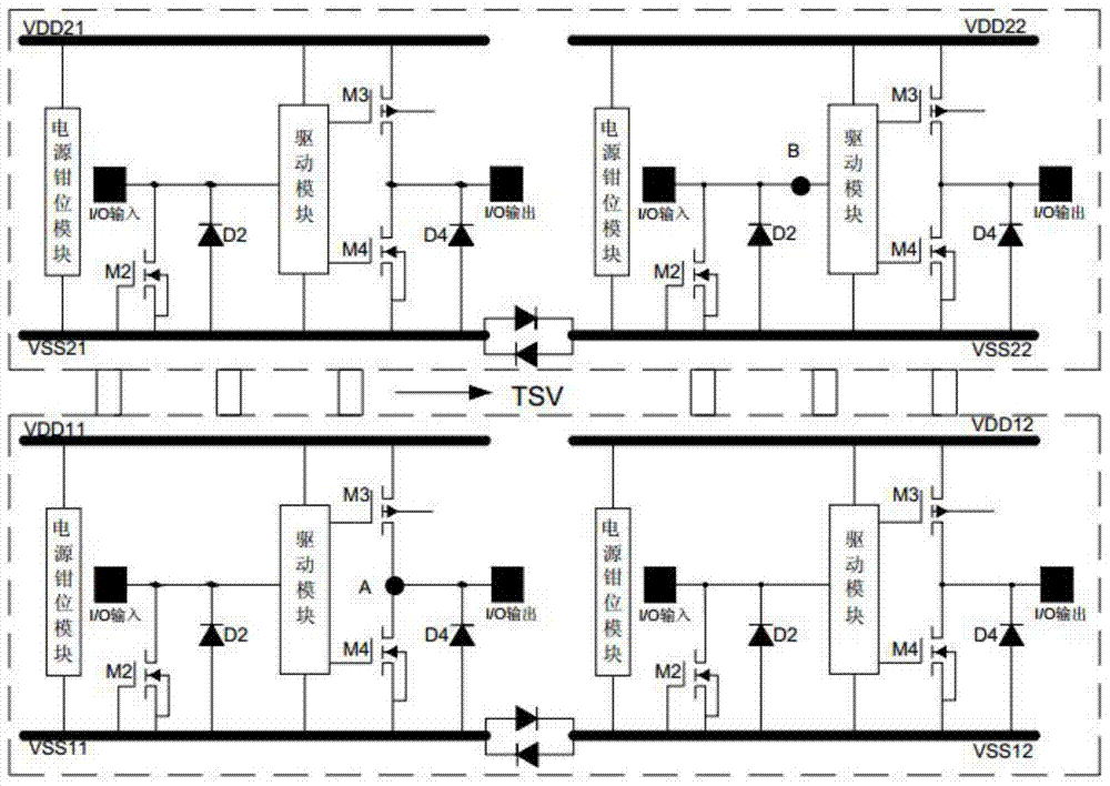
[0061] The embodiment one is image 3 The circuit in is modified to form Figure 4 the circuit described.
[0062] Specifically, in Embodiment 1, the drain of transistor M3 is changed from being connected to the power supply voltage VDD to connecting the drain of transistor M3 to the VDD bus, and the electrostatic protection circuit further includes a transistor M5; wherein, the gate of transistor M5 is connected to the power supply voltage VDD is connected, the source of transistor M5 is connected to the gate of transistor M3, and the drain of transistor M5 is connected to the VDD bus.
[0063] In the embodiment of the present invention, the transistor M5 is a PMOS transistor, and the drive module can be divided into various drive units according to needs, such as Figure 4 As shown, the driving module is a logic circuit and a pre-stage driving circuit, and the pre-stage driving circuit is connected to the power supply voltage VDD through the diode D6.
[0064] In the embo...
PUM
 Abstract
Description
Claims
Application Information
 - R&D Engineer
- R&D Manager
- IP Professional
- Industry Leading Data Capabilities
- Powerful AI technology
- Patent DNA Extraction
Browse by: Latest US Patents, China's latest patents, Technical Efficacy Thesaurus, Application Domain, Technology Topic, Popular Technical Reports.
© 2024 PatSnap. All rights reserved.Legal|Privacy policy|Modern Slavery Act Transparency Statement|Sitemap|About US| Contact US: help@patsnap.com