
Reaction device for preparing transverse nanowire net on silicon electrode

A technology of a reaction device and a nanowire mesh, which is applied in the field of semiconductor nanowire preparation, can solve the problems of unsatisfactory nanowires and complicated nanowire preparation equipment, and achieves the effect of saving processes and reducing costs.

Active Publication Date: 2015-08-26
CHONGQING INST OF GREEN & INTELLIGENT TECH CHINESE ACADEMY OF SCI
View PDF8 Cites 2 Cited by
  • Summary
  • Abstract
  • Description
  • Claims
  • Application Information

AI Technical Summary

Problems solved by technology

[0011] In view of the shortcomings of the prior art described above, the purpose of the present invention is to provide a reaction device for preparing a lateral nanowire network on a silicon electrode, which is used to solve the problem that the preparation equipment of the prior art nanowires is relatively complicated and only obtained Nanowires are not ideal

Method used


Image

  • Reaction device for preparing transverse nanowire net on silicon electrode
  • Reaction device for preparing transverse nanowire net on silicon electrode
  • Reaction device for preparing transverse nanowire net on silicon electrode

Examples


Embodiment Construction

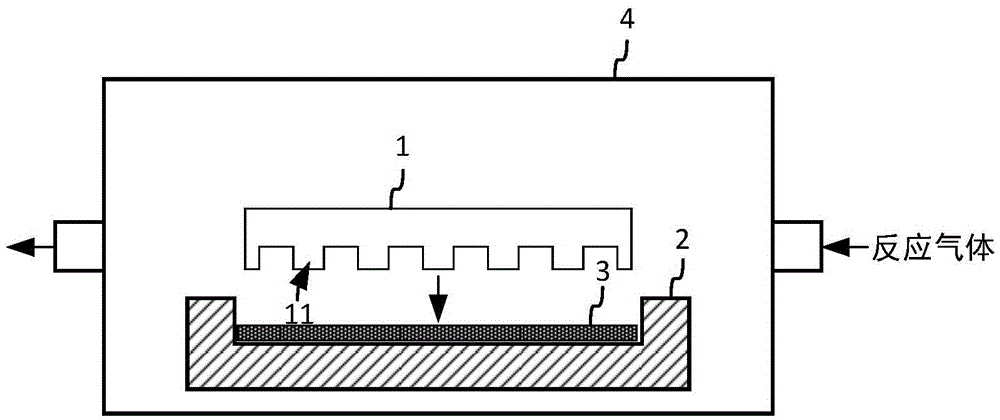
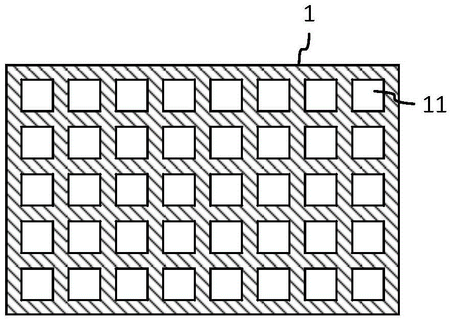
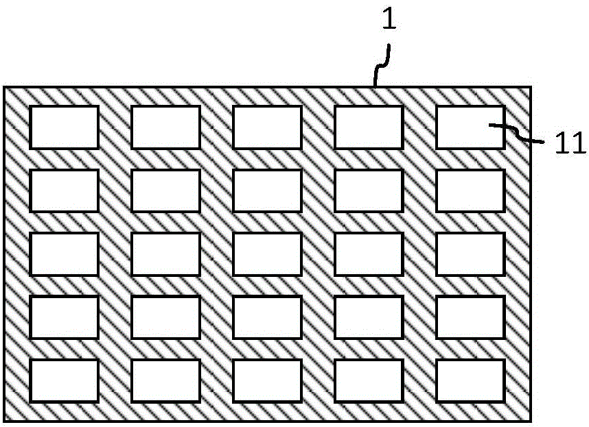
[0025] The implementation of the present invention will be illustrated by specific specific examples below, and those skilled in the art can easily understand other advantages and effects of the present invention from the contents disclosed in this specification.

[0026] It should be noted that the structures, proportions, sizes, etc. shown in the drawings attached to this specification are only used to match the content disclosed in the specification, for those who are familiar with this technology to understand and read, and are not used to limit the implementation of the present invention. Limiting conditions, so there is no technical substantive meaning, any modification of structure, change of proportional relationship or adjustment of size, without affecting the effect and purpose of the present invention, should still fall within the scope of the present invention. The disclosed technical content must be within the scope covered. At the same time, terms such as "upper"...


PUM

PropertyMeasurementUnit
Heightaaaaaaaaaa

Abstract

The invention discloses a reaction device for preparing a transverse nanowire net on a silicon electrode. The reaction device comprises a silicon substrate which is prepared with periodic nanometer silicon columns on a surface, a boat for containing chemical reactant raw material, and a tubular vacuum furnace into which reaction gas is input, wherein the silicon substrate and the boat are placed in the tubular vacuum furnace, and the silicon substrate is horizontally placed above the boat, and the surface of the silicon substrate, which is prepared with the periodic nanometer silicon columns, faces the chemical reactant raw material in the boat. By downwardly arranging a silicon electrode substrate growth plane whose surface is prepared with the periodic nanometer silicon columns in the boat containing the chemical reactants, the reaction device for preparing transverse nanowire net on the silicon electrode controls the nanowire net which is transversely grown to form a nanowire net bridge circuit and does not need gold-plating as a catalyst, thereby saving working procedures and reducing cost.

Description

technical field [0001] The invention relates to the field of semiconductor nanowire preparation, in particular to a reaction device for preparing a lateral nanowire network on a silicon electrode. Background technique [0002] Scientific research shows that nanowire nets can improve the specific surface area and electrical properties of semiconductor materials, so the research on how to prepare nanowire nets is also constantly being studied. There are two main types of existing technologies for preparing nanowire networks: [0003] First, in the published document 1 (see the end of the article for details), a method for preparing a horizontal single-arm carbon nanotube network (Carbon nanotube nanonets) circuit by post-processing method is disclosed, which can be found in figure 1 , the method is to distribute the nanotubes on the surface of the silicon substrate of silicon dioxide, and then use the method of ultraviolet exposure photolithography to coat the metal film as t...

Claims


Application Information

Patent Timeline
IPC IPC(8): B81C1/00
Inventor 陆文强何培培石彪冯双龙李昕王亮宋金会
Owner CHONGQING INST OF GREEN & INTELLIGENT TECH CHINESE ACADEMY OF SCI
Features
  • Generate Ideas
  • Intellectual Property
  • Life Sciences
  • Materials
  • Tech Scout
  • Unparalleled Data Quality
  • Higher Quality Content
  • 60% Fewer Hallucinations
Learn More