Display device
A technology for display equipment and display panels, applied in the directions of light guides, optics, instruments, etc., can solve the problems of lower transmittance than expected and lower brightness of display panels, etc., to improve the incidence of light, reduce the generation of relative displacement, and reduce relative displacement. Effect
- Summary
- Abstract
- Description
- Claims
- Application Information
AI Technical Summary
Problems solved by technology
Method used
Image
Examples
Embodiment 1
[0028] Embodiment 1: Stereoscopic display device
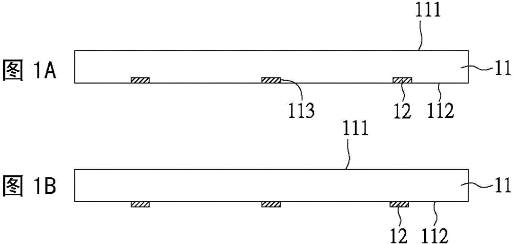
[0029] First, if Figure 1A As shown, a light guide mother board 11 is provided, which is a glass substrate. Wherein, the light guide motherboard 11 has a first surface 111 and an opposite second surface 112 , and the second surface 112 is further provided with a plurality of scattering stripe patterns 12 . Here, each scattering stripe pattern 12 is embedded in a groove 113 of the light guide motherboard 11 . However, in other embodiments, the scattering stripe pattern 12 can be directly disposed on the second surface 112 of the light guide motherboard 11, such as Figure 1B shown.
[0030] Here, the material of the scattering stripe pattern 12 is not particularly limited, and can be any material that can reduce the occurrence of total reflection. For example, the material of the scattering stripe pattern 12 may be a composite material formed of titanium dioxide and ink or photoresist; however, the invention is not limited ...
Embodiment 2
[0048] Embodiment 2: flat display device
[0049] The light guide plate prepared in Example 1 above can also be applied to the flat display device of this embodiment; the difference is that the flat display device of this embodiment does not need to be provided with the scattering stripe pattern of Example 1, but is used in the light guide plate. The second surface 112 of the light board 1 forms a dot pattern (not shown); meanwhile, the pixel unit 43 of the display panel 4 does not need to be composed of a plurality of sub-pixel units.
[0050] Here, the light guide plate of the present embodiment has the same features as the light guide plate of the embodiment 1, so details are not repeated here.
[0051] In addition, the display device of the aforementioned embodiment 1 and embodiment 2 is not particularly limited, it can be a liquid crystal display device or an organic light emitting diode display device; and it can be applied to monitors, mobile phones, notebook computers,...
PUM
| Property | Measurement | Unit |
|---|---|---|
| refractive index | aaaaa | aaaaa |
| water absorption | aaaaa | aaaaa |
| refractive index | aaaaa | aaaaa |
Abstract
Description
Claims
Application Information


