
Method for manufacturing silicon carbide semiconductor device

A manufacturing method and semiconductor technology, applied in semiconductor devices, semiconductor/solid-state device testing/measurement, electric solid-state devices, etc., can solve problems such as increase in forward characteristic resistance, stacking fault expansion, etc., to prevent increase in manufacturing costs, The effect of good positive characteristics

Active Publication Date: 2015-08-26
MITSUBISHI ELECTRIC CORP
View PDF7 Cites 0 Cited by
  • Summary
  • Abstract
  • Description
  • Claims
  • Application Information

AI Technical Summary

Problems solved by technology

[0002] Conventionally, in silicon carbide semiconductor devices having a pn junction and including a bipolar operation structure, when a current is made to flow in the forward direction of the pn junction, there is a problem that due to the recoupling current of the pn junction, the crystal defects leading to the expansion of stacking faults and, as a result, an increase in the resistance of the forward characteristic

Method used


Image

  • Method for manufacturing silicon carbide semiconductor device
  • Method for manufacturing silicon carbide semiconductor device
  • Method for manufacturing silicon carbide semiconductor device

Examples


no. 1 Embodiment approach

[0019]

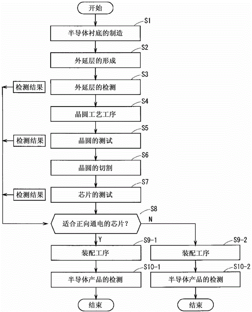
[0020] figure 1 It is a flowchart showing the outline of the method of manufacturing a silicon carbide semiconductor device according to the present embodiment of the present invention. In this embodiment, a silicon carbide semiconductor MOSFET (Metal-Oxide-Semiconductor Field-Effect Transistor) is assumed as an example of a semiconductor device.

[0021] First, a substrate manufacturing step is performed in which a semiconductor substrate of the first conductivity type is manufactured (step S1). Specifically, a silicon carbide substrate was produced by a modified sublimation method (modified Lely method). In addition, it is also possible to purchase commercially available silicon carbide substrates that have already been manufactured and used in subsequent steps.

[0022] At this time, in order to suppress the expansion of stacking faults generated when the current flows to the pn junction in the forward direction (forward energization), it is desirable to produc...

no. 2 Embodiment approach

[0069]

[0070] Figure 4 It is a flowchart showing the outline of the method of manufacturing a silicon carbide semiconductor device according to this embodiment. exist Figure 4 Since steps S1 to S7 are the same as those in the first embodiment, detailed description thereof will be omitted.

[0071] After step S7, a mounting process is performed in which a semiconductor chip is fixed in a case or a module, and wiring is formed (step S9).

[0072] Then, a product inspection step is performed in which initial characteristics of the assembled silicon carbide semiconductor device (product) are inspected (step S10 ). The detection result is stored in a predetermined storage area as detection result data.

[0073] Then, a screening step is performed in which, in the silicon carbide semiconductor device (product), it is detected whether or not there is deterioration when the pn junction is forwardly energized (step S11 ). Specifically, the presence or absence of an increase i...


PUM


Abstract

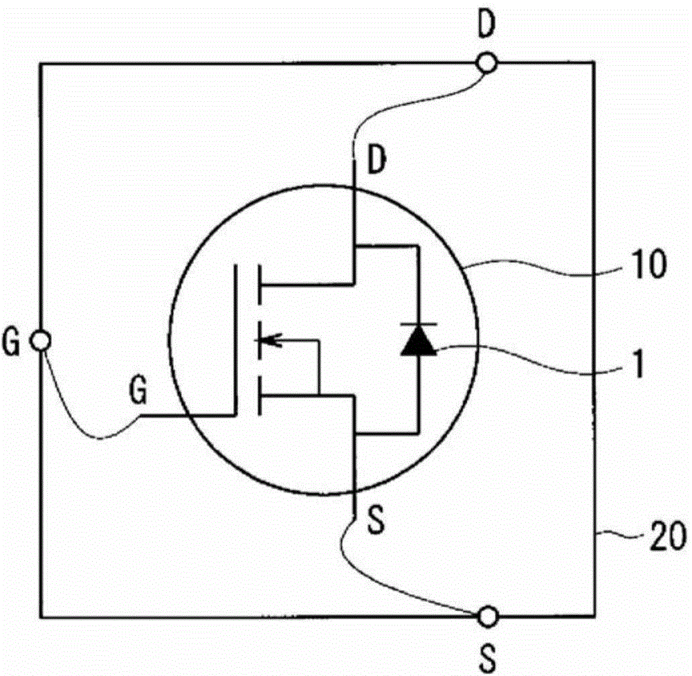
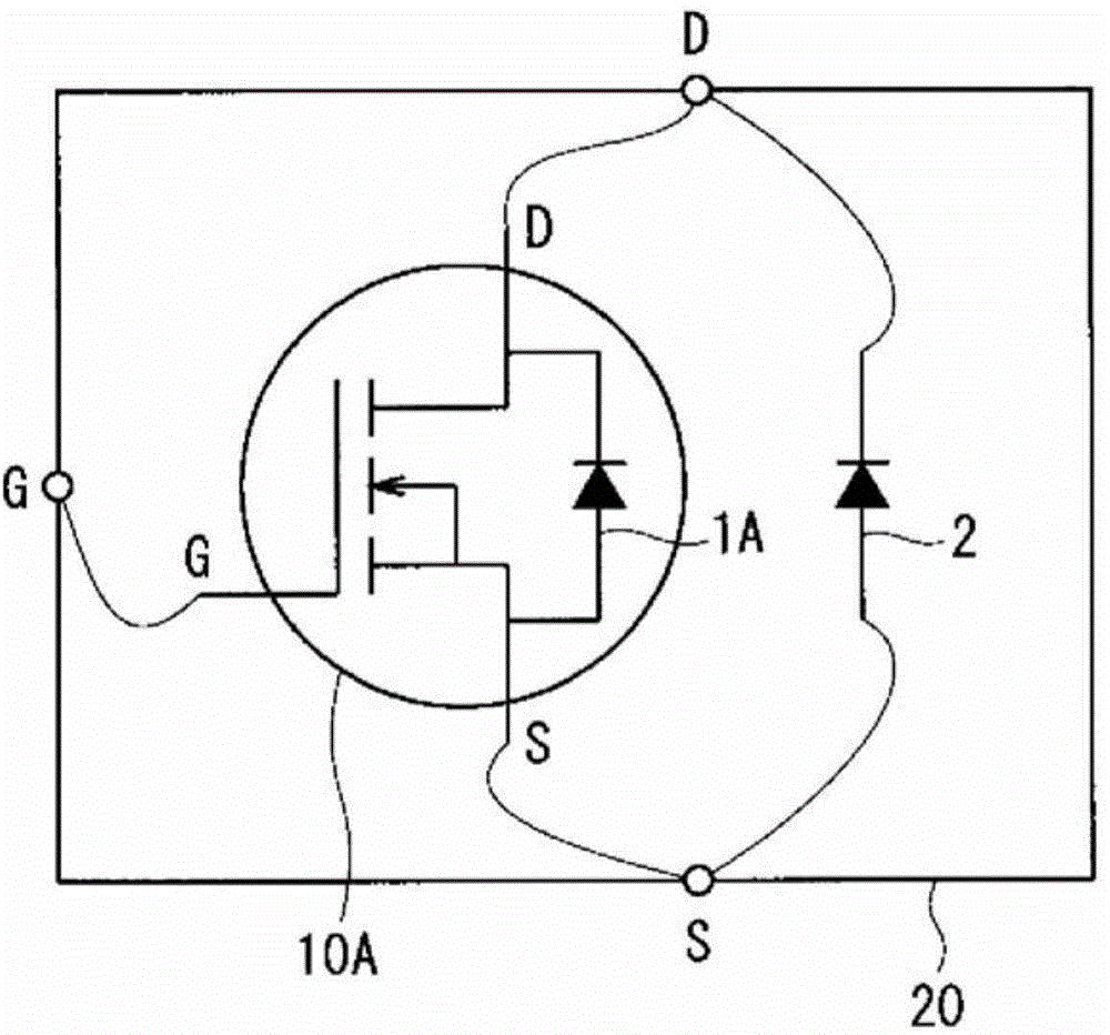
It is an objective of the invention to provide a method for manufacturing a silicon carbide semiconductor device capable of preventing an increase in the manufacturing cost of a chip while favorably maintaining the forward-direction characteristics of a semiconductor device. The invention includes (a) a step of inspecting the forward-direction electric conduction characteristics of body diodes (1) and (1A) as element structures, (b) a step of classifying the body diode (1) and the body diode (1A) into a first group and a second group on the basis of the inspection results in the step (a), and (c) a step of manufacturing a silicon carbide semiconductor MOSFET (10) using the body diode (1) in the first group and manufacturing a silicon carbide semiconductor MOSFET (10A) using the body diode (1A) in the second group. The first group is suitable for forward-direction electric conduction, and the second group is not suitable for forward-direction electric conduction. The silicon carbide semiconductor MOSFET (10) requires forward-direction electric conduction, and the silicon carbide semiconductor MOSFET (10A) does not require forward-direction electric conduction.

Description

technical field [0001] The present invention relates to a method of manufacturing a silicon carbide semiconductor device including a bipolar operation structure in a silicon carbide semiconductor element. Background technique [0002] Conventionally, in silicon carbide semiconductor devices having a pn junction and including a bipolar operation structure, when a current is made to flow in the forward direction of the pn junction, there is a problem that due to the recoupling current of the pn junction, the Crystal defects lead to the expansion of stacking faults, and as a result, the resistance of the forward characteristic increases. Crystal defects that cause stacking faults are formed during the manufacturing process of a semiconductor substrate and an epitaxial layer on the semiconductor substrate. [0003] For example, Patent Document 1 proposes a method of observing the positional coordinates of crystal defects in the substrate in advance with an optical microscope or...

Claims


Application Information

Patent Timeline
Patent Type & Authority Applications(China)
IPC IPC(8): H01L21/66
CPCH01L2924/0002H01L22/20H01L25/18H01L22/14H01L29/1608H01L29/7805H01L2924/00
Inventor 杉本博司中村卓誉
Owner MITSUBISHI ELECTRIC CORP
Learn More