Ga2O3 Schottky diode device structure and manufacturing method thereof

A Schottky diode and device structure technology, applied in the field of microelectronics, can solve the problems of enhanced parasitic effects and increased parasitic capacitance, and achieve the effects of stable physical and chemical properties, reduced peak electric field, and improved breakdown voltage

Active Publication Date: 2017-06-23
XIDIAN UNIV
View PDF7 Cites 21 Cited by
  • Summary
  • Abstract
  • Description
  • Claims
  • Application Information

AI Technical Summary

Problems solved by technology

However, since the field plate structure introduces the dielectric layer, it will inevitably lead to the enhancement of the parasitic effect, resulting in an increase in the parasitic capacitance

Method used


Image

  • Ga2O3 Schottky diode device structure and manufacturing method thereof
  • Ga2O3 Schottky diode device structure and manufacturing method thereof

Examples


Embodiment 1

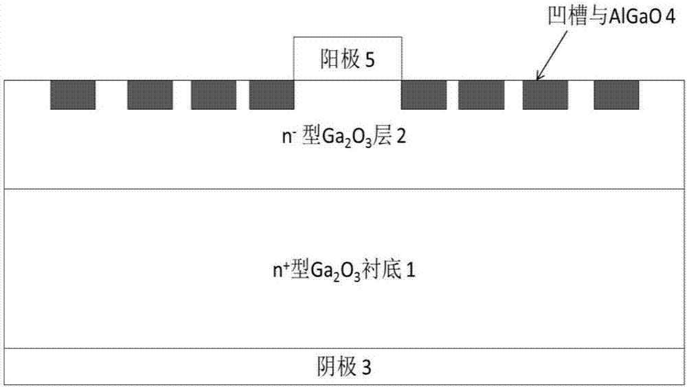
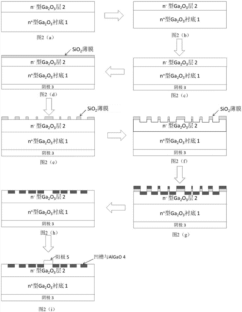
[0030] Embodiment 1, making Schottky diodes with groove number M=4, groove depth of 30 nm, width of 2 μm, and groove pitch increasing in order of 0.3 μm.

[0031] Step 1, cleaning, such as figure 2 (a).

[0032] Ga has been epitaxially grown on the substrate 2 o 3 The samples were cleaned organically under the conditions of ultrasonication of acetone solution for 5 minutes, ultrasonic solution of ethanol solution for 5 minutes, and then cleaned with deionized water, and then put into HF:H 2 Erosion was carried out in a solution of O=1:1 for 50s, and finally cleaned with flowing deionized water and dried with high-purity nitrogen.

[0033] Step 2, etch, such as figure 2 (b).

[0034] Put the cleaned sample face down into the ICP etching reaction chamber, and slightly etch the lower surface of the substrate. The process conditions are: the power of the upper electrode is 100W, the power of the lower electrode is 10W, the pressure of the reaction chamber is 30Pa, BCl 3 Th...

Embodiment 2

[0049] Example 2, Schottky diodes with groove number M=5, groove depth of 40 nm, width of 2.5 μm, and groove pitches increasing by 0.4 μm were fabricated.

[0050] Step one, cleaning.

[0051] The specific implementation of this step is the same as step 1 of Embodiment 1.

[0052] Step two, etching.

[0053] The specific implementation of this step is the same as that of step 2 in Embodiment 1.

[0054] Step 3, preparing the cathode electrode.

[0055] The specific implementation of this step is the same as that of step 3 in Embodiment 1.

[0056] Step 4, deposit SiO 2 mask.

[0057] The specific implementation of this step is the same as step 4 of Embodiment 1.

[0058] Step five, remove the SiO in the groove etching area 2 mask.

[0059] The specific implementation of this step is the same as that of step 5 in Embodiment 1.

[0060] Step six, etching grooves.

[0061] Put the sample into the ICP etching reaction chamber, the upper electrode power is 100W, the lower...

Embodiment 3

[0068] Embodiment 3, making Schottky diodes with groove number M=6, groove depth of 50 nm, width of 3 μm, and groove pitch increasing by 0.5 μm.

[0069] Step A, wash.

[0070] The specific implementation of this step is the same as step 1 of Embodiment 1.

[0071] Step B, etching.

[0072] The specific implementation of this step is the same as that of step 2 in Embodiment 1.

[0073] Step C, preparing a cathode electrode.

[0074] The specific implementation of this step is the same as that of step 3 in Embodiment 1.

[0075] Step D, depositing SiO 2 mask.

[0076] The specific implementation of this step is the same as step 4 of Embodiment 1.

[0077] Step E, removing the SiO in the groove etching area 2 mask.

[0078] The specific implementation of this step is the same as that of step 5 in Embodiment 1.

[0079] Step F, etching grooves.

[0080] Put the sample into the ICP etching reaction chamber, the upper electrode power is 100W, the lower electrode power is ...


PUM


Abstract

The invention discloses a Ga2O3 Schottky diode device structure and a manufacturing method thereof, and mainly aims at solving the problems that a present Schottky diode device is low in reverse breakdown voltage and the parasitic capacitance in a field plate structure is high. The Ga2O3 Schottky diode device structure comprises a cathode electrode, a heavily-doped n type Ga2O3 substrate, a low-doped n type Ga2O3 epitaxial layer and an anode electrode from bottom to top; Schottky contact is formed in the part where the anode makes contact with the epitaxial layer, the cathode and the substrate make ohmic contact, grooves are distributed separately in the low-doped n type Ga2O3 epitaxial layer, intervals of grooves are increased progressively within the range of 0.3 to 0.5 micron, the first groove is positioned below the edge of the anode, the distance between the last groove and the first groove ranges from 10 to 15 micron, and AlGaO layers in which the Al component is greater than 20% are grown in an epitaxial manner in the grooves respectively. Thus, the reverse breakdown voltage is improved, the parasitic capacitance is reduced, positive characteristic is kept unchanged, and the structure and manufacturing method thereof can be used for high-speed integration circuits and microwave technologies.

Description

technical field [0001] The invention belongs to the technical field of microelectronics, and in particular relates to a Schottky diode, which is used in high-speed integrated circuits and microwave technology. Background technique [0002] Schottky diodes are manufactured on the principle that a Schottky barrier is formed by the contact between a metal and a semiconductor, and the Schottky barrier acts as a rectifier. Compared with pn junction diodes, Schottky diodes have the advantages of lower turn-on voltage and faster switching speed, so they are widely used in high-speed integrated circuits, microwave technology and other fields. However, since the electric field of the Schottky diode is mainly concentrated in the edge region of the Schottky contact, when the electric field in this region reaches the breakdown field strength of the material, the device is prone to breakdown in this region, while the electric field in the rest of the region is smaller than that of the ma...

Claims


Application Information

Patent Timeline
Patent Type & Authority Applications(China)
IPC IPC(8): H01L29/872H01L29/06H01L21/34
CPCH01L29/0615H01L29/66969H01L29/872H01L29/24
Inventor 冯倩邢翔宇韩根全李翔方立伟黄璐张进成郝跃
Owner XIDIAN UNIV
Why Eureka
Try Eureka