Method for welding component pin and apparatus thereof

A welding method and component technology, which is applied to the assembly of printed circuits, electrical components, welding equipment, etc. with electrical components, can solve problems such as poor welding, difficult energy control, and burnt PCB boards, so as to increase size adaptability and reduce interference and damage, avoiding the effect of high costs

Active Publication Date: 2015-09-23
HANS LASER TECH IND GRP CO LTD
View PDF11 Cites 11 Cited by
  • Summary
  • Abstract
  • Description
  • Claims
  • Application Information

AI Technical Summary

Problems solved by technology

[0003] In the prior art, the laser heating position of laser wire feeding welding is on the copper clad layer and the plug-in on the PCB, and the wire feeding position is on the copper clad layer on the PCB. Since most of the laser is irradiated on the pins of the plug-in , the temperature rises quickly; a small part of the copper clad layer on the PCB board, the temperature of the copper clad layer on the PCB board is relatively low, so the pins of the plug-in are easily oxidized, making the welding poor; the laser is reflected on the surface of the solder joint formed by welding, which will cause Burn the PCB board; and the size of the pad and the clearance between the round hole and the plug-in are very demanding
The existing solution is to use optical path shaping to achieve uniform heating through annular light spots, but the cost is very high
[0004] At the same time, when the existing PCB board and the plug-in are soldered, when there are protruding electronic components around, wave soldering cannot be used. The existing method is to use an automatic soldering machine or manual soldering. The existing automatic soldering machine is contact soldering. Space limitations; there are hidden dangers of instability in manual welding due to human factors and labor intensity.
[0005] The laser wire-feed soldering used in the prior art accumulates less heat in the PCB board during welding, and the energy is difficult to control during the melting and spreading of the solder, and it is easy to burn out the PCB board

Method used


Image

  • Method for welding component pin and apparatus thereof
  • Method for welding component pin and apparatus thereof

Examples


Embodiment Construction

[0027] In order to facilitate the understanding of the present invention, the present invention will be described more fully below with reference to the associated drawings. Preferred embodiments of the invention are shown in the accompanying drawings. However, the present invention can be embodied in many different forms and is not limited to the embodiments described herein. On the contrary, these embodiments are provided to make the understanding of the disclosure of the present invention more thorough and comprehensive.

[0028] Unless otherwise defined, all technical and scientific terms used herein have the same meaning as commonly understood by one of ordinary skill in the technical field of the invention. The terms used herein in the description of the present invention are for the purpose of describing specific embodiments only, and are not intended to limit the present invention.

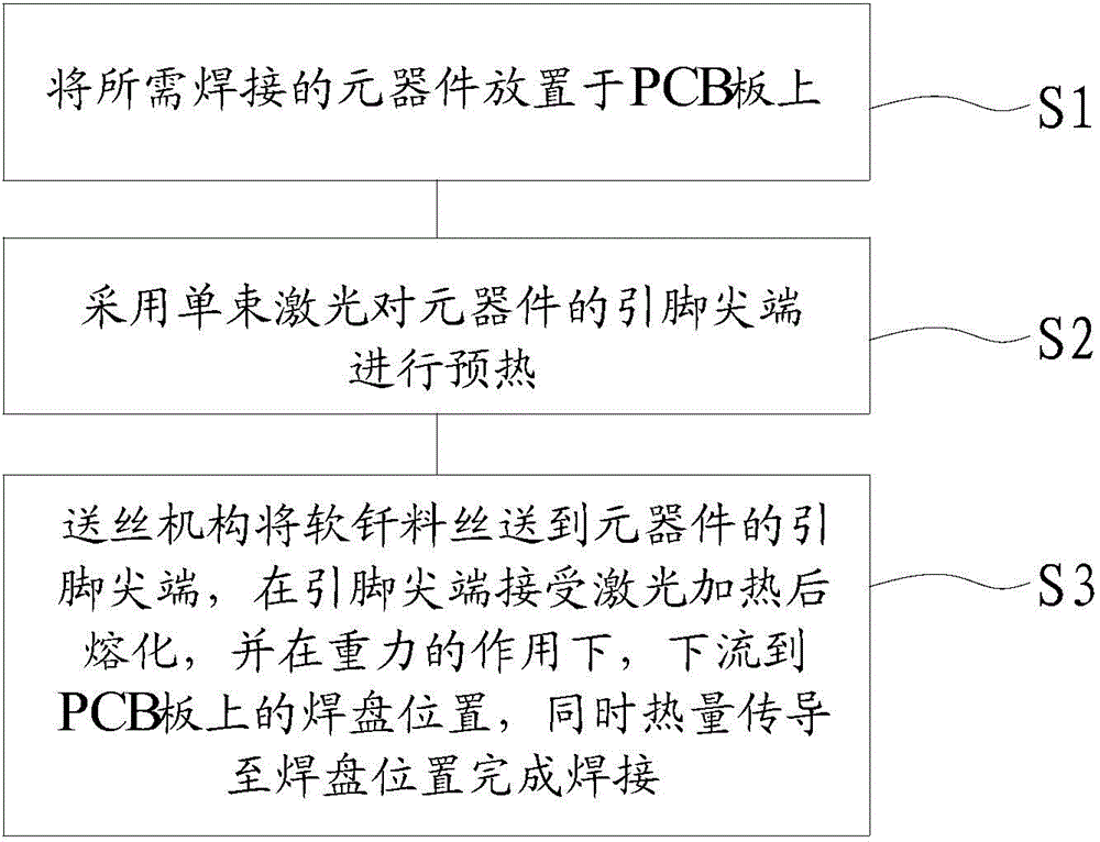
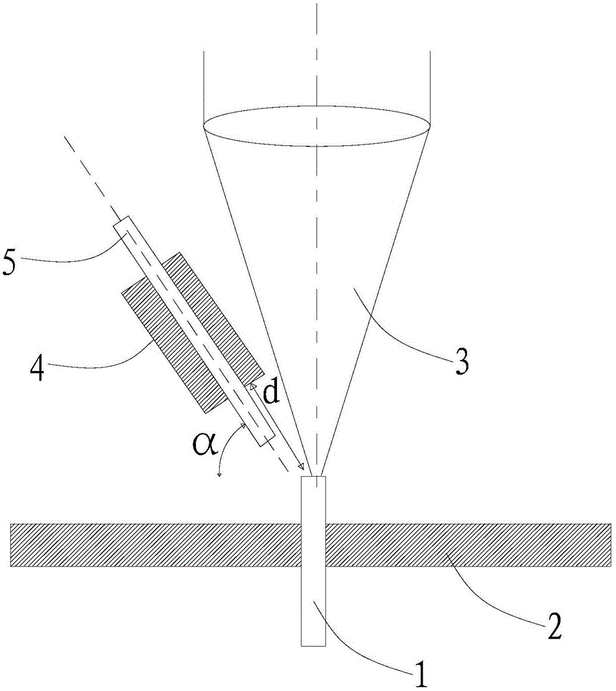
[0029] refer to Figure 1 ~ Figure 2 As shown, a welding method for component pins ...


PUM


Abstract

The invention relates to the field of welding technology, and discloses a method for welding a pin of a component and an apparatus thereof. The method herein comprises welding the component pin to a PCB board by using laser and a wire feeder, wherein the laser refers to a single beam laser. During welding, the laser supplies heat to the tip end of the component pin, and the wire feeder delivers the wire to the tip end of the component pin. According to the invention, the laser supplies heat to the tip end of the component pin instead of a coated copper layer on the PCB board, and the wire feeder delivers the wire to the tip end of the component pin instead of the coated copper layer on the PCB board. Thus, the method herein is applicable to welding pins of all plug-in types of components with no concerns of the morphology of the cross section or the size of the cross section area, or factors like heat radiation property of the coated copper layer. The method herein has the advantages of short pre-heating time, simple modulation, and a wide range of application.

Description

technical field [0001] The invention relates to the field of welding technology, and more specifically, relates to a welding method and device for component pins. Background technique [0002] With the rapid development of electronic manufacturing technology, the increasingly widespread application of IT industry and the promotion of micro-processing technology, especially in the situation of a substantial increase in the consumption of various personal communication and entertainment equipment such as mobile phones, notebook computers, MP3 / MP4, and digital cameras , the products of the electronic and electrical industry are increasingly developing in the direction of high integration, intelligence, miniaturization and portability. On the other hand, the direction of product development puts forward higher requirements for manufacturing technology. In order to achieve the requirements of smaller product volume and lighter weight, the internal structures of various electronic...

Claims


Application Information

Patent Timeline
Patent Type & Authority Applications(China)
IPC IPC(8): B23K26/21B23K26/60H05K3/34
CPCB23K26/20B23K2101/42H05K3/3405
Inventor 朱宝华肖华高云峰
Owner HANS LASER TECH IND GRP CO LTD
Why Eureka
Try Eureka