Manufacture method and structure of TFT substrate

A manufacturing method and substrate technology, applied to electrical components, electrical solid devices, circuits, etc., can solve the problems of image flicker coupling voltage response time, charging rate deviation, liquid crystal capacitance and storage capacitance deviation from simulation results, and thickness reduction. To achieve the effect of shortening the production cycle, reducing risks and improving quality

Active Publication Date: 2015-09-23
TCL CHINA STAR OPTOELECTRONICS TECH CO LTD
View PDF3 Cites 6 Cited by
  • Summary
  • Abstract
  • Description
  • Claims
  • Application Information

AI Technical Summary

Problems solved by technology

[0014] In the manufacturing method of the above-mentioned TFT substrate, when performing the first dry etching process in step 3, the parts of the non-TFT region of the amorphous silicon layer 510 and the N-type heavily doped amorphous silicon layer 520 have been completely etched away (such as image 3 shown), when performing the second dry etching process in step 6, the gate insulating layer 400 is not shielded above the part of the non-TFT region, so a part is often etched away, so that the gate insulating layer 400 400 The thickness of the part located in the non-TFT area is reduced, causing damage (such as Image 6 shown), according to practical experience, the etching amount of the second dry etching process is usually results in thinning of the gate insulating layer 400 This will cause the actual liquid crystal capacitance and storage capacitance (MII capacitance) to deviate from the simulation results, resulting in image flicker (Flicker), and deviations in parameters such as coupling voltage (Vft), response time, and charging rate.

Method used


Image

  • Manufacture method and structure of TFT substrate
  • Manufacture method and structure of TFT substrate
  • Manufacture method and structure of TFT substrate

Examples


Embodiment Construction

[0060] In order to further illustrate the technical means adopted by the present invention and its effects, the following describes in detail in conjunction with preferred embodiments of the present invention and accompanying drawings.

[0061] see Figure 7 , the present invention at first provides a kind of manufacture method of TFT substrate, comprises the following steps:

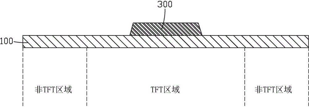
[0062] Step 1, such as Figure 8 As shown, a substrate 1 is provided, and a TFT region and a non-TFT region are provided on the substrate 1; a first metal layer is deposited on the substrate 1, and the first metal layer is patterned by a photolithography process to form a Gate 3 in the middle of the TFT area.

[0063] Specifically, in step 1, the physical vapor deposition method is used to deposit the first metal layer, and the material of the first metal layer is copper, aluminum, or molybdenum.

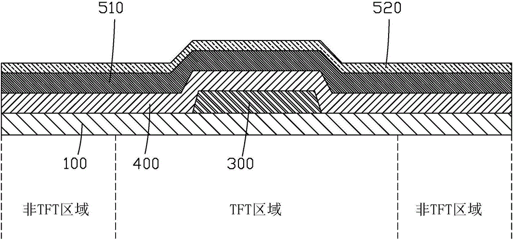
[0064] Step 2, such as Figure 9 As shown, a gate insulating layer 4 , an amorphous silicon layer 51 ,...


PUM


Abstract

The invention provides a manufacture method and structure of a TFT substrate. According to the manufacture method of the TFT substrate, part, placed in a non-TFT area, of an amorphous silicon layer (51) is reserved in certain thickness in the first dry etching process, a back channel (515) is formed in the second dry etching process, the reserved amorphous silicon layer (51) in the non-TFT area, and thus, a grid insulating layer (4) is prevented from damage in the second dry etching process. The quality of the TFT substrate is improved, the risk of quality problems is reduced, the etching amount in the first dry etching process is reduced, the etching time is reduced, the production period is shortened, and the factory capacity is improved. The TFT substrate provided by the invention is simple in structure, the grid insulating layer (4) is complete without damage, and the quality of an LCD can be improved.

Description

technical field [0001] The invention relates to the field of display technology, in particular to a manufacturing method and structure of a TFT substrate. Background technique [0002] With the development of display technology, liquid crystal displays (Liquid Crystal Display, LCD) and other flat display devices are widely used in mobile phones, televisions, personal digital assistants, digital Various consumer electronic products such as cameras, notebook computers, and desktop computers have become the mainstream of display devices. [0003] Most of the liquid crystal display devices currently on the market are backlight liquid crystal displays, which include a liquid crystal display panel and a backlight module. The working principle of the liquid crystal display panel is to place liquid crystal molecules between two parallel glass substrates. There are many vertical and horizontal small wires between the two glass substrates. The direction of the liquid crystal molecule...

Claims


Application Information

Patent Timeline
Patent Type & Authority Applications(China)
IPC IPC(8): H01L27/12H01L29/10H01L29/06
Inventor 孙博
Owner TCL CHINA STAR OPTOELECTRONICS TECH CO LTD
Why Eureka
Try Eureka