Formation method of semiconductor structure

A semiconductor and gate structure technology, applied in the field of semiconductor structure formation, can solve the problems of increasing gate parasitic capacitance, shrinking semiconductor device size, affecting transistor performance, etc.

Active Publication Date: 2017-12-01
SEMICON MFG INT (SHANGHAI) CORP
View PDF4 Cites 0 Cited by
  • Summary
  • Abstract
  • Description
  • Claims
  • Application Information

AI Technical Summary

Problems solved by technology

[0003] The gate of the transistor is made of conductive materials such as polysilicon or metal, and the insulating dielectric material is filled between adjacent gates, so that parasitic capacitance is formed between adjacent gates, which affects the performance of the transistor
In addition, a metal plug located in the insulating dielectric material is also formed on the surface of the source and drain of the transistor, the metal plug is isolated from the gate by an insulating dielectric material, and the gap between the gate and the metal plug is It will also form parasitic capacitance, affecting the performance of the transistor
[0004] With the improvement of chip integration, the size of semiconductor devices shrinks, and the distance between adjacent gates decreases, so that the parasitic capacitance of the gate becomes larger, which further affects the performance of the transistor.
[0005] The performance of existing transistors needs to be further improved

Method used


Image

  • Formation method of semiconductor structure
  • Formation method of semiconductor structure
  • Formation method of semiconductor structure

Examples


Embodiment Construction

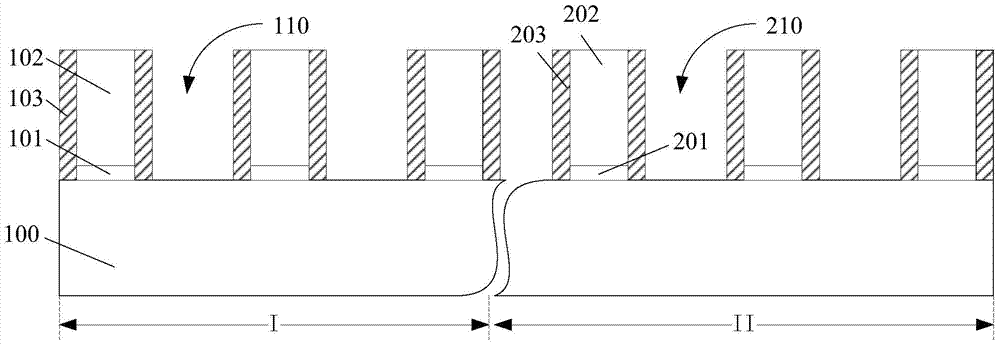
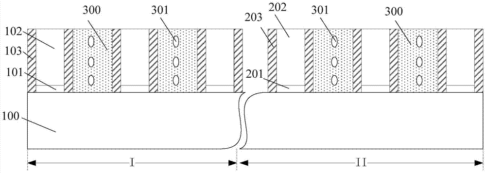
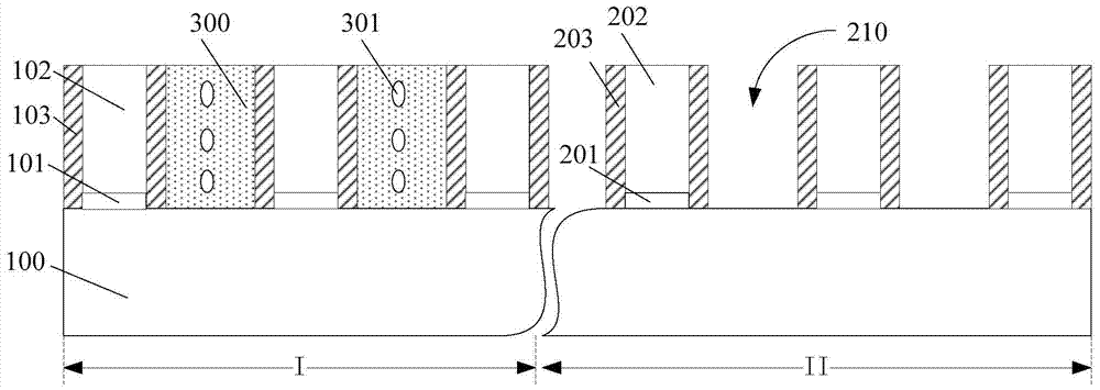
[0032] As mentioned in the background art, in existing integrated circuits, the distances between the gates of adjacent transistors and between the gates and the metal plugs are small, so large parasitic capacitances are formed.

[0033] The operating speed of devices in the core area of ​​the integrated circuit is inversely proportional to the parasitic capacitance, and the core area may be devices such as processors and memories. The greater the parasitic capacitance, the lower the operating speed of the device. The core area is a sensitive area for parasitic capacitance, and the device in the core area generally has a low operating voltage, and the compactness of the dielectric layer between adjacent gates is not high. . However, in the peripheral area of ​​the integrated circuit, such as the input or output transistor, the parasitic capacitance has little influence on the performance of the transistor, and the peripheral area is an insensitive area of ​​the parasitic capac...


PUM


Abstract

A method for forming a semiconductor structure, comprising: providing a semiconductor substrate, the semiconductor substrate has a first region, a plurality of protruding first gate structures are formed on the first region, adjacent to the first gate structure There is a first groove between them; hydrophobic treatment is carried out on the surface of the side wall of the first groove, so that the first groove has a hydrophobic side wall; a first medium is formed in the first groove by a fluid chemical vapor deposition process layer, the reactant used in the fluid chemical vapor deposition process is a hydrophilic substance, and under the action of the hydrophobic sidewall, there is an air gap in the first dielectric layer. The method can reduce the dielectric coefficient of the first dielectric layer and reduce the parasitic capacitance between adjacent first gate structures.

Description

technical field [0001] The invention relates to the technical field of semiconductors, in particular to a method for forming a semiconductor structure. Background technique [0002] In the field of existing integrated circuits and semiconductor manufacturing, transistors are one of the basic components constituting semiconductor devices, and are therefore widely used. With the integration of integrated circuits and the miniaturization of semiconductor devices, the performance of transistors has an increasingly significant impact on integrated circuits. Among the factors affecting the performance of the transistor, the gate parasitic capacitance of the transistor has a great influence on the performance of the transistor. [0003] The gate of the transistor is made of conductive materials such as polysilicon or metal, and insulating dielectric materials are filled between adjacent gates, so that parasitic capacitance is formed between adjacent gates, which affects the perfor...

Claims


Application Information

Patent Timeline
Patent Type & Authority Patents(China)
IPC IPC(8): H01L21/28H01L29/423
Inventor 三重野文健
Owner SEMICON MFG INT (SHANGHAI) CORP
Why Eureka
Try Eureka