Eureka AIR delivers breakthrough ideas for toughest innovation challenges, trusted by R&D personnel around the world.

Manufacturing method and structure of current limiting control diode

A technology of current limiting control and manufacturing method, which is applied in semiconductor/solid-state device manufacturing, electrical components, circuits, etc. It can solve the problems of unsatisfactory manufacturing methods or structures, achieve safety and reliability, quickly limit current, and avoid damage.

Active Publication Date: 2015-09-30
贵州煜立电子科技有限公司
View PDF4 Cites 0 Cited by
  • Summary
  • Abstract
  • Description
  • Claims
  • Application Information

AI Technical Summary

Problems solved by technology

Therefore, the manufacturing methods or structures of existing semiconductor high-power diode devices are still not ideal enough to meet the needs of use.

Method used


Image

  • Manufacturing method and structure of current limiting control diode
  • Manufacturing method and structure of current limiting control diode
  • Manufacturing method and structure of current limiting control diode

Examples


Embodiment

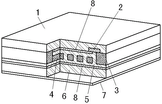
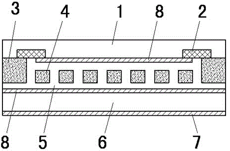
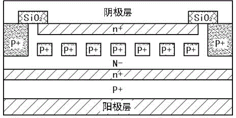
[0026] In specific implementation, use such as Figure 1~3 As shown, different effects can be obtained by changing the structure of the P+ buried layer 4 . It can be made into a series of products with different physical characteristics of current limiting control. The P+ buried layer 4 can be realized by ion influx or buried layer diffusion process.

[0027] The specific method is: diffuse a layer of n+ layer on the silicon substrate with P+ impurities, perform N- epitaxy on the n+ layer, diffuse P+ impurities on the N- epitaxial layer, and then perform the second epitaxy to form a P+ buried layer. The diffusion wall of P+ impurity is diffused around the epitaxial layer, and the P+ buried layer is connected with the P+ diffusion wall. The whole forms a Figure 6 The bottom PN junction and multi-N-channel parallel connection self-adjustable JFET field effect transistor structure, the field effect transistor is similar to a multi-N-channel JFET with a common gate (P+buri...


PUM


Abstract

The invention discloses a manufacturing method and a structure of a current limiting control diode. An N- epitaxial layer arranged on a P+ silicon lining layer form a group of mutually parallel strip-shaped P+ impurities by adopting an iron injection process or an embedded layer diffusion process; then, epitaxial coverage is carried out on the P+ impurities; the strip-shaped P+ impurities are buried in the N- epitaxial layer to form a P+ burying layer; in addition, a P+ diffusion wall is also formed on the periphery of the N- epitaxial layer by adopting the iron injection process or the embedded layer diffusion process; the P+ diffusion wall is communicated with the two ends of all of the P+ embedded layer; the current limiting control on the diode is realized through the opening and the closing of a plurality of parallelly connected N channels formed in the epitaxial layer by a plurality of P+ embedded layers. The method and the structure have the advantages that the self current limiting control protection concept is adopted; the current limiting control valve value is set, so that when the current value of a diode device exceeds the current threshold, the self protection capability of the electronic device is realized; the change speed of a PN junction consumption layer is very fast; the fast current limiting effect can be achieved; the damage to the diode is avoided; the safety of electronic equipment is reliably guaranteed.

Description

technical field [0001] The invention relates to a manufacturing method and structure of a current-limiting control diode, belonging to the technical field of semiconductor devices. technical background [0002] The safety and reliability of semiconductor high-power diode devices is the most concerned issue in the field of electronic equipment. The current method to solve this problem is mainly to expand the current and power capacity of the device itself, or to take various protective measures. These methods are not economical, and will bring new unreliable factors (the reliability of various protection measures themselves needs to be guaranteed), and loopholes in protection measures are inevitable. Therefore, the manufacturing method or structure of the existing semiconductor high-power diode device is still not ideal enough to meet the needs of use. Contents of the invention [0003] The object of the present invention is to provide a manufacturing method and structure...

Claims


Application Information

Patent Timeline
Patent Type & Authority Applications(China)
IPC IPC(8): H01L29/861H01L21/329
CPCH01L29/6609H01L29/861
Inventor 刘桥
Owner 贵州煜立电子科技有限公司
Why Eureka
Eureka Blog
Learn More