GaAs-based pHEMT device and preparation method therefor

A device and barrier layer technology, applied in semiconductor/solid-state device manufacturing, semiconductor devices, electrical components, etc., to achieve the effect of low process difficulty and improved gate-to-drain breakdown voltage

Active Publication Date: 2015-10-07
CHENGDU HIWAFER SEMICON CO LTD
View PDF4 Cites 4 Cited by
  • Summary
  • Abstract
  • Description
  • Claims
  • Application Information

AI Technical Summary

Problems solved by technology

[0005] However, with the continuous advancement of semiconductor technology, improving the gate-drain breakdown voltage has gradually entered the bottleneck. For example, the working voltage and breakdown voltage of the 0.15μm process are generally difficult to exceed 8V and 20V, and the continuous improvement of RF front-end performance requirements requires The operating voltage of GaAs-based pHEMT devices continues to increase, which also means that GaAs-based pHEMT devices are required to have a higher gate-drain breakdown voltage, and the existing process can no longer meet this requirement

Method used


Image

  • GaAs-based pHEMT device and preparation method therefor
  • GaAs-based pHEMT device and preparation method therefor
  • GaAs-based pHEMT device and preparation method therefor

Examples


Embodiment Construction

[0020] The following will clearly and completely describe the technical solutions in the embodiments of the present invention with reference to the accompanying drawings in the embodiments of the present invention. Obviously, the described embodiments are only some, not all, embodiments of the present invention. Based on the embodiments of the present invention, all other embodiments obtained by persons of ordinary skill in the art without making creative efforts belong to the protection scope of the present invention.

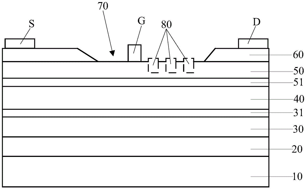
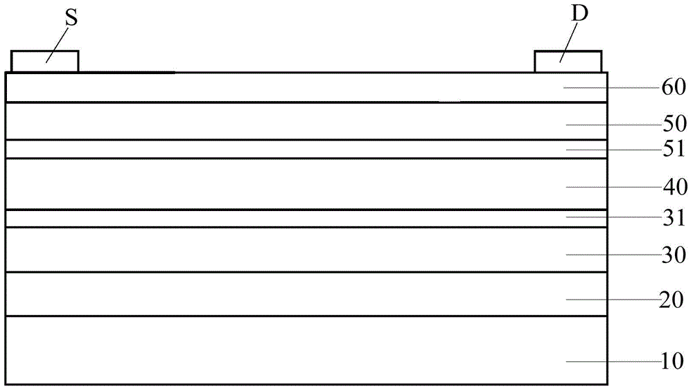
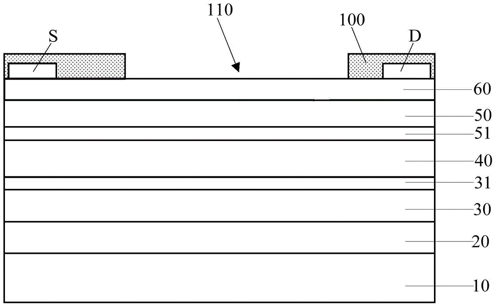
[0021] see figure 1 , is a schematic cross-sectional view of a GaAs-based pHEMT device according to an embodiment of the present invention. The GaAs-based pHEMT device of this embodiment includes a GaAs substrate 10, a buffer layer 20, a first AlGaAs barrier layer 30, an InGaAs channel layer 40, a second AlGaAs barrier layer 50, and N + - GaAs layer 60 . The first AlGaAs barrier layer 30 and the InGaAs channel layer 40 form a two-dimensional electron gas 31 ...


PUM


Abstract

The invention provides a GaAs-based pHEMT device and a preparation method therefor. The device comprises a GaAs substrate, a buffer layer, a first AlGaAs barrier layer, an InGaAs channel layer, a second AlGaAs barrier layer and a N<+>-GaAs layer. The channel layer and two barrier layers form two-dimensional electron gases respectively. A source electrode and a drain electrode are formed on the N<+>-GaAs layer. A recessed groove exposed from the second AlGaAs barrier layer is arranged between the source electrode and the drain electrode. A grid electrode is formed in the recessed groove. A nodal region with a high dielectric constant is arranged in a recessed groove between the grid electrode and the drain electrode. The nodal region with a high dielectric constant is embedded from the upper surface of the second AlGaAs barrier layer and extends into the interior. The distance of the source electrode to the grid electrode is equal to the distance of the drain electrode to the grid electrode. The transverse width of the recessed groove between the grid electrode and the drain electrode is more than the transverse width of the recessed groove between the grid electrode and the source electrode. The grid-drain breakdown voltage can be raised under a condition that device performances are not affected.

Description

technical field [0001] The invention relates to the technical field of semiconductor manufacturing, in particular to a GaAs-based pHEMT device and a preparation method thereof. Background technique [0002] GaAs (gallium arsenide) is the most important and widely used semiconductor material among III-V compound semiconductors. The electron mobility in GaAs is 6 times that of Si (silicon), and its electron peak drift speed is 2 times that of Si. Therefore, GaAs devices have the characteristics of high frequency, high speed, low power consumption, low noise, and monolithic integration. [0003] GaAs-based pHEMT device is a relatively mature three-terminal device among GaAs devices. It has the advantages of superior microwave and high-speed performance, relatively simple process, and stability. It is the focus of people's research. Output power and reliability are two important performance indicators of GaAs-based pHEMT devices. When the GaAs-based pHEMT device works in the s...

Claims


Application Information

Patent Timeline
Patent Type & Authority Applications(China)
IPC IPC(8): H01L29/778H01L29/20H01L21/335H01L21/266H01L29/41
CPCH01L21/2654H01L21/266H01L29/20H01L29/41H01L29/66462H01L29/778
Inventor 陈一峰
Owner CHENGDU HIWAFER SEMICON CO LTD
Why Eureka
Try Eureka