Manufacturing method of semiconductor device and manufacturing method of triple mode integrate-insulated gate bipolar transistor (TI-IGBT)

A manufacturing method and semiconductor technology, which is applied in the manufacture of TI-IGBTs and semiconductor devices, can solve problems such as the rate of warping and fragmentation, avoid processing, reduce the probability of warping and fragmentation, and increase the yield Effect

Inactive Publication Date: 2015-10-14
JIANGSU CAS JUNSHINE TECH +1
View PDF5 Cites 7 Cited by
  • Summary
  • Abstract
  • Description
  • Claims
  • Application Information

AI Technical Summary

Problems solved by technology

[0005] In view of this, the present invention provides a manufacturing method of a semiconductor device and an IGBT manufacturing method

Method used


Image

  • Manufacturing method of semiconductor device and manufacturing method of triple mode integrate-insulated gate bipolar transistor (TI-IGBT)
  • Manufacturing method of semiconductor device and manufacturing method of triple mode integrate-insulated gate bipolar transistor (TI-IGBT)
  • Manufacturing method of semiconductor device and manufacturing method of triple mode integrate-insulated gate bipolar transistor (TI-IGBT)

Examples


Embodiment Construction

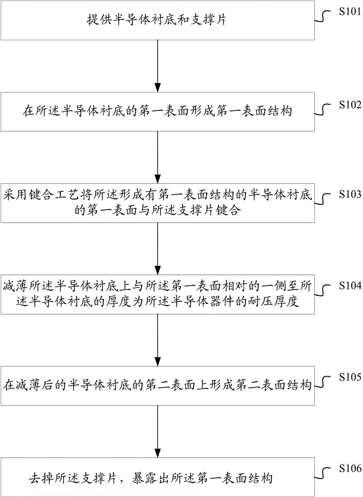
[0041] As mentioned in the background art section, in the prior art, during the process of manufacturing semiconductor devices, the semiconductor substrate is prone to problems of warpage and high fragmentation rate.

[0042] The inventor found that the reason for the above phenomenon is that the semiconductor device has a withstand voltage thickness, usually its thickness (less than 100 μm) is relatively thin, and in order to reduce the difficulty of the process, the functional area with complex process is usually fabricated on a thicker semiconductor substrate , and then thinning the semiconductor substrate to the withstand voltage thickness required by the semiconductor device, and then manufacturing a relatively simple functional region. However, since the thickness of the thinned semiconductor substrate is very thin, the problem of warping or fragmentation of the semiconductor substrate is prone to occur during the multi-process process.

[0043] Based on this, the invent...


PUM


Abstract

The present invention provides a manufacturing method of a semiconductor device and a manufacturing method of a TI-IGBT. The manufacturing method of the semiconductor device comprises the steps of manufacturing a first surface structure on one surface of a semiconductor substrate, then bonding a supporting piece on the surface structure, and then thinning one side of the semiconductor substrate relative to the supporting piece, and finally manufacturing a second surface structure in the thinned surface. By the above manufacturing method, the first surface structure is manufactured on the semiconductor substrate before thinning, and the second surface structure is manufactured on the thinned piece bonded with the supporting piece, namely, the two surface structures are both manufactured on the substrate having a thicker thickness, thereby avoiding processing the thinner semiconductor substrate, reducing the warping and break probability of the semiconductor substrate, and improving the yield of the semiconductor device.

Description

technical field [0001] The invention relates to the field of semiconductor devices, and more specifically relates to a method for manufacturing a semiconductor device and a method for manufacturing a TI-IGBT. Background technique [0002] Power semiconductor devices are mainly used for high-power (usually tens to thousands of amps in current and hundreds of volts in voltage) electronic devices in power conversion and control circuits of power equipment. The power semiconductor device includes IGBT (Insulated Gate Bipolar Transistor, insulated gate bipolar transistor), VDMOS (Vertical Double diffused MOS, vertical double diffused metal-oxide field effect transistor), FRD (Fast Recovery Diode, fast recovery diode) , GTO (Gate Turn-Off Thyristor, the gate can turn off the thyristor), IEGT (Injection Enhanced Gate Transistor, electron injection enhanced gate transistor), IGCT (Integrated Gate-Commutated Thyristor, integrated gate commutated thyristor), MTO ( MOS Controlled Gate...

Claims


Application Information

Patent Timeline
IPC IPC(8): H01L21/02H01L21/683H01L21/331
Inventor 张文亮朱阳军卢烁今
Owner JIANGSU CAS JUNSHINE TECH
Why Eureka
Try Eureka