Method for forming fin type field effect transistor

A fin field effect and transistor technology, which is applied in semiconductor/solid-state device manufacturing, electrical components, circuits, etc., can solve the problems that the electrical parameters of the fin field effect transistor cannot meet the requirements, and it is difficult to accurately control the thickness of the gate dielectric layer. , to achieve the effect of easy thickness

Active Publication Date: 2015-10-14
SEMICON MFG INT (SHANGHAI) CORP
View PDF4 Cites 34 Cited by
  • Summary
  • Abstract
  • Description
  • Claims
  • Application Information

AI Technical Summary

Problems solved by technology

[0004] In the prior art, the fin field effect transistors in the core area and the peripheral area are generally formed at the same time, but in the process of forming the fin field effect transistors in the core area and the peripheral area at the same time, it is difficult to accurately control the fin field effect transistors in the peripheral area The thickness of the gate dielectric layer of the effect transistor causes the electrical parameters of the fin field effect transistor in the peripheral region to fail to meet the requirements

Method used


Image

  • Method for forming fin type field effect transistor
  • Method for forming fin type field effect transistor
  • Method for forming fin type field effect transistor

Examples


Embodiment Construction

[0031] As mentioned in the background art, in the prior art, when transistors in the core region and the peripheral region are formed at the same time, it is difficult to accurately control the gate dielectric layer of the transistor in the peripheral region, which easily leads to unsatisfactory device performance.

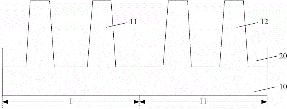
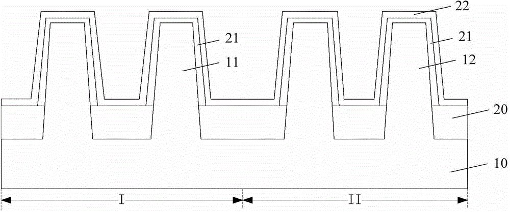
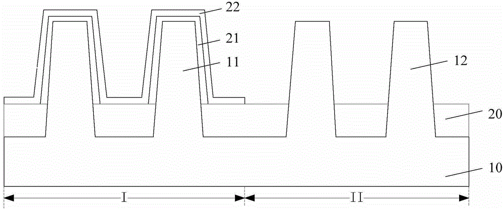
[0032] Figure 1 to Figure 4 A formation process of a gate dielectric layer of a fin field effect transistor according to an embodiment is provided.

[0033] Please refer to figure 1 , provide a semiconductor substrate 10, the semiconductor substrate 10 includes a first region I and a second region II, a first fin 11 is formed on the first region I, and a second fin is formed on the second region II. Fin 12 , a dielectric layer 20 is formed on the surface of the semiconductor substrate 10 , and the surface of the dielectric layer 20 is lower than the surfaces of the first fin 11 and the second fin 12 .

[0034] The first region I is used to form peripheral circu...


PUM


Abstract

A method for forming a fin type field effect transistor comprises the steps of providing a semiconductor substrate which comprises a first region and a second region, wherein a first fin part is formed on the first region and a second fin part is formed on the second region, and an insulating layer is formed on the semiconductor substrate; forming a barrier layer on the second fin part; forming a first pseudo gate structure on the first region; forming a second pseudo gate structure on the second region, wherein the second pseudo gate structure is arranged on the surface of the barrier layer and bestrides the second fin part; forming a dielectric layer which is level with the first pseudo gate structure and the second pseudo gate structure on the semiconductor substrate; eliminating the first pseudo gate structure for forming a first groove which is exposed from the surface of the first fin part, and eliminating the second pseudo gate structure for forming a second groove which is exposed from the barrier layer on the second fin part; and forming a first gate structure in the first groove, and forming a second gate structure in the second groove. The method of the invention can be used for accurately adjusting the gate dielectric layer thickness of the fin type field effect transistor which is formed on different regions.

Description

technical field [0001] The invention relates to the technical field of semiconductors, in particular to a method for forming a fin field effect transistor. Background technique [0002] With the continuous development of semiconductor process technology, the process node is gradually reduced, the traditional gate dielectric layer is getting thinner, and the leakage of transistors is increasing, which causes problems such as waste of power consumption of semiconductor devices. In order to solve the above problems, the prior art provides a solution of replacing the polysilicon gate with a metal gate. Among them, the "gate last" process is a main process for forming high-K metal gate transistors. However, when the feature size of the device is further reduced, even if the gate-last process is adopted, the structure of the conventional MOS field effect transistor can no longer meet the requirements for device performance. Fin field effect transistor (Fin FET) is obtained as a m...

Claims


Application Information

Patent Timeline
Patent Type & Authority Applications(China)
IPC IPC(8): H01L21/336
Inventor 谢欣云
Owner SEMICON MFG INT (SHANGHAI) CORP
Why Eureka
Try Eureka