Semiconductor device and manufacturing method thereof

A manufacturing method and semiconductor technology, which can be used in the manufacture of semiconductor/solid-state devices, semiconductor devices, electrical components, etc., can solve problems such as poor adhesion, and achieve the effect of improving the height of the potential barrier

Active Publication Date: 2015-10-14
TOYODA GOSEI CO LTD
View PDF3 Cites 5 Cited by
  • Summary
  • Abstract
  • Description
  • Claims
  • Application Information

AI Technical Summary

Problems solved by technology

However, there is a problem that metals such as platinum (Pt) and palladium (Pd) with a large work function have poor adhesion to GaN

Method used


Image

  • Semiconductor device and manufacturing method thereof
  • Semiconductor device and manufacturing method thereof
  • Semiconductor device and manufacturing method thereof

Examples


no. 1 Embodiment approach

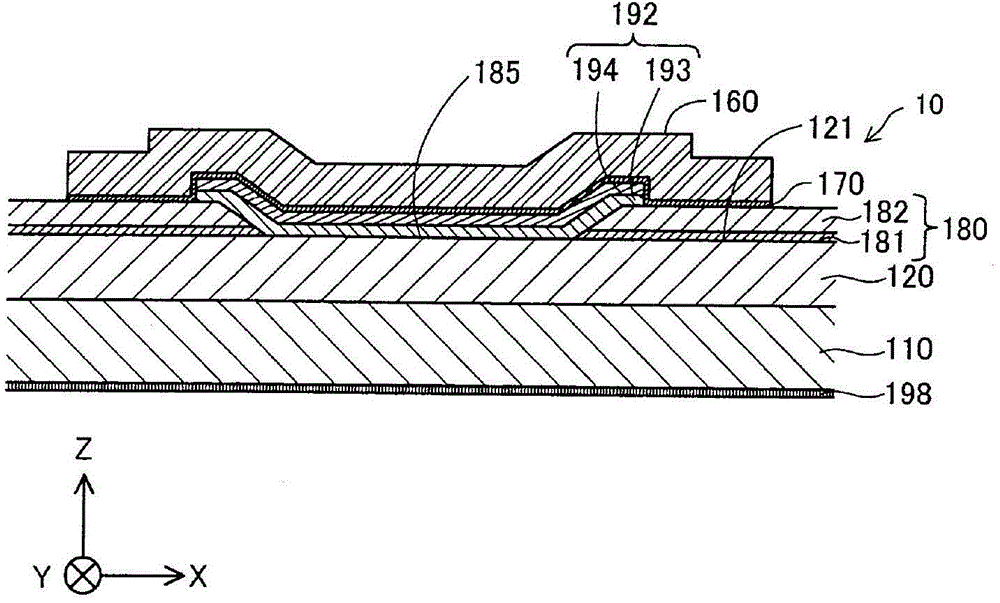
[0051] A-1. Configuration of semiconductor device

[0052] figure 1 It is a cross-sectional view schematically showing the configuration of the semiconductor device 10 in the first embodiment. figure 1 The diagram in the center has XYZ axes perpendicular to each other.

[0053] figure 1 The XYZ axis, the X axis is from figure 1 The left side of the paper faces the right side of the paper, the +X axis direction is toward the right side of the paper, and the -X axis direction is toward the left side of the paper. figure 1 The XYZ axis, the Y axis is from figure 1 The front of the paper faces the axis of the back of the paper, the direction of the +Y axis is the direction of the back of the paper, and the direction of the -Y axis is the direction of the front of the paper. figure 1 The XYZ axis, the Z axis is from figure 1 The lower side of the paper faces the upper side of the paper, the +Z axis direction is toward the upper side of the paper, and the -Z axis direc...

no. 2 Embodiment approach

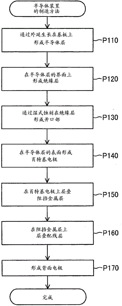
[0093] B-1. Manufacturing method of semiconductor device

[0094] Figure 9 It is a process diagram showing another manufacturing method of the semiconductor device 10 . In the present embodiment, as a manufacturing method, after forming the Schottky electrode 192 in the manufacturing method of the first embodiment (step P140 ), heat treatment is performed in step P145 . By heat treatment after forming the Schottky electrode 192, the nickel layer 193 is sequentially divided from the semiconductor layer 120 side into (i) a layer with less than 0.1% palladium and a film thickness of 50 nm or more, and (ii) a layer with 0.1% or more palladium. . Here, the layer with less than 0.1% of palladium corresponds to the "third layer" in the means for solving the problems, and the layer with 0.1% or more of palladium corresponds to the "fourth layer" in the means for solving the problems.

[0095] B-2. Evaluation of barrier height between semiconductor layer and Schottky electrode befo...


PUM


Abstract

The present invention provides a technology for improving the barrier height of an electrode layer and a semiconductor layer. The semiconductor device comprises a semiconductor layer which is formed by semiconductors, and an electrode layer, wherein at least one part of the semiconductor layer is in Schottky connection with the electrode layer; the electrode layer comprises a first layer and a second layer successively from the semiconductor layer side; the first layer is mainly formed by nickel, and the film thickness is 50-200nm; the second layer is mainly formed by at least one metal of palladium, platinum and iridium; and the film thickness of the second layer is greater than the film thickness of the first layer.

Description

technical field [0001] The present invention relates to semiconductor devices. Background technique [0002] GaN-based semiconductor devices including one or more semiconductor layers mainly formed of gallium nitride (GaN) are known as semiconductor devices (semiconductor devices, semiconductor elements). A GaN-based semiconductor device functions as a Schottky Barrier Diode (SBD) (for example, Patent Document 1). [0003] In GaN-based Schottky barrier diodes, in order to enable high-voltage operation, a technique for increasing the barrier height between the Schottky electrode and the semiconductor layer is desired. The greater the work function of the metal used for the Schottky electrode, the higher the barrier height can be. However, there is a problem that metals such as platinum (Pt) and palladium (Pd) having a large work function have poor adhesion to GaN. [0004] Patent Document 1 discloses the following manufacturing method in order to increase the barrier heigh...

Claims


Application Information

Patent Timeline
Patent Type & Authority Applications(China)
IPC IPC(8): H01L29/872H01L29/47H01L21/329H01L21/28
CPCH01L21/28581H01L29/1608H01L29/2003H01L29/401H01L29/402H01L29/475H01L29/66212H01L29/778H01L29/872H01L21/324H01L29/66143
Inventor 长谷川一也冈彻田中成明
Owner TOYODA GOSEI CO LTD
Why Eureka
Try Eureka