Method based on femtosecond laser technology for peeling GaN film and sapphire substrate

A sapphire substrate, femtosecond laser technology, applied in semiconductor devices, electrical components, circuits, etc., can solve the problems of GaN thin film vulnerable to damage, low yield, low efficiency, etc., to overcome vulnerability to damage, precision and efficiency Increased, uniform temperature effect

Inactive Publication Date: 2015-10-28
WUHAN UNIV +1
View PDF4 Cites 23 Cited by
  • Summary
  • Abstract
  • Description
  • Claims
  • Application Information

AI Technical Summary

Problems solved by technology

[0003] Aiming at the defects such as low efficiency, low yield, and easy damage of GaN thin film in the method of laser stripping sapphire substrate, combined with femtosecond laser technology, the present invention proposes a method for stripping GaN thin film and sapphire based on femtosecond laser technology method

Method used


Image

  • Method based on femtosecond laser technology for peeling GaN film and sapphire substrate

Examples


Embodiment 1

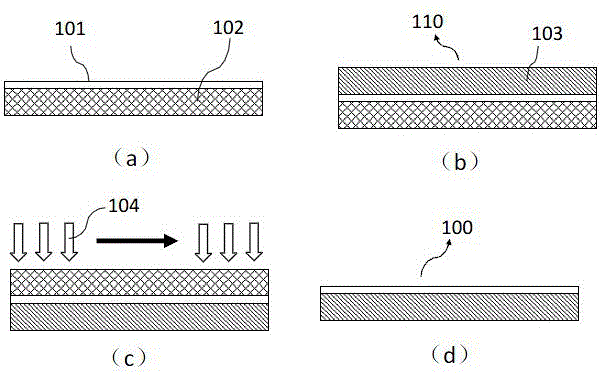
[0040] figure 1 It is a process flow chart of the GaN thin film and sapphire substrate peeling method based on femtosecond laser technology. Use MOCVD technology to deposit and prepare a GaN film 101 with a thickness of 1um on a sapphire substrate 102 with a good surface treatment (both sides of the sapphire substrate is polished), such as figure 1 (a); The target substrate 103 (silicon substrate) is directly bonded to the GaN thin film 101 to obtain a three-layer structure 110 of sapphire / GaN / target substrate, such as figure 1 As shown in (b): adjust the spot size of the femtosecond laser beam 103, and focus on the interface between the GaN film 101 and the sapphire substrate 102, scan from the edge of the three-layer structure 110 for laser irradiation until it is completed, as figure 1 As shown in (c): the three-layer structure 110 is heated to 30°C (the melting point of metal Ga), and the sapphire 102 is removed to obtain the double-layer structure 100 of the GaN film 101...

Embodiment 2

[0043] The difference from Embodiment 1 is that the bonding method between the target substrate 103 (silicon substrate) and the GaN thin film 101 is adhesive bonding.

Embodiment 3

[0045] The difference from Example 1 is that the Ga removal treatment is a femtosecond laser vaporization treatment.


PUM

PropertyMeasurementUnit
thicknessaaaaaaaaaa

Abstract

The invention discloses a method based on a femtosecond laser technology for peeling a GaN thin film and a sapphire substrate, and the method belongs to the field of LED and power device chips. The method comprises the steps of: (1) growing the GaN thin film on the sapphire substrate by adopting chemical vapor deposition; (2) bonding a target substrate on the GaN thin film to obtain a sapphire / GaN / target substrate; (3) carrying out scanning radiation on the upper surface of the sapphire substrate by adopting femtosecond laser from the edge of the sapphire / GaN / target substrate; (4) and heating the sapphire / GaN / target substrate to not lower than 30 DEG C and removing the sapphire substrate to obtain a bilayer structure of the GaN / target substrate. The method provided by the invention has the advantages that: the method is a cold processing method, the temperature in the GaN thin film before and after femtosecond laser radiation is even and has no obvious change, the thermal stress influence on the GaN thin film is effectively reduced, and the laser peeling quality is improved; and the method increases the efficiency and yield of peeling the sapphire substrate, and overcomes the defect that the GaN thin film is liable to damage.

Description

technical field [0001] The invention relates to the field of LEDs and power device chips, in particular to a method for peeling off a GaN thin film and a sapphire substrate based on femtosecond laser technology. Background technique [0002] In recent years, among the big family of semiconductor LEDs and other power devices, the development of GaN-based LEDs is the most rapid and noticeable. With its direct bandgap and excellent optoelectronic properties, GaN-based semiconductor materials have made many major technological breakthroughs in the preparation of thin-film preparation, crystal growth and other optoelectronic devices. GaN-based semiconductor materials are therefore known as the driving force for the development of the lighting field. However, it is difficult to directly grow a thick layer of GaN, so most of the cheap sapphire is used as a heterogeneous substrate at present. However, the lattice mismatch between sapphire and GaN material is large, resulting in a h...

Claims


Application Information

Patent Timeline
Patent Type & Authority Applications(China)
IPC IPC(8): H01L21/683H01L33/00
CPCH01L21/6835H01L33/007H01L2221/68386
Inventor 刘胜付兴铭刘亦杰郑怀沈沁宇
Owner WUHAN UNIV
Why Eureka
Try Eureka