Nitride semiconductor light-emitting element

A technology of nitride semiconductors and light-emitting elements, which is applied in semiconductor devices, semiconductor lasers, electrical components, etc., can solve problems such as insufficient light output, high carrier concentration, and low luminous efficiency, and achieve the effect of improving luminous efficiency

Active Publication Date: 2015-10-28
STANLEY ELECTRIC CO LTD
View PDF8 Cites 10 Cited by
  • Summary
  • Abstract
  • Description
  • Claims
  • Application Information

AI Technical Summary

Problems solved by technology

[0003] However, light-emitting elements using semiconductors have problems of weaker light output and lower luminous efficiency than gas light sources such as deuterium gas lamps and mercury gas lamps.
[0004] As the cause of insufficient light output of the semiconductor light-emitting element, it can be cited that in the nitride semiconductor light-emitting element, the effective mass of electrons is small compared with holes, and the carrier concentration is high, so that electrons pass through the active layer ( region), overflowing to the p-type layer, resulting in a reduction in luminous efficiency
The overflow of electrons to the p-type layer leads to a further decrease in luminous efficiency and an increase in heat generation under high injection current conditions.
As a result, the light output reaches a limit, and it is difficult to obtain a light output corresponding to the amount of injected carriers.

Method used


Image

  • Nitride semiconductor light-emitting element
  • Nitride semiconductor light-emitting element
  • Nitride semiconductor light-emitting element

Examples


Embodiment approach (1

[0108] (Other embodiment (1): other configurations of the active layer)

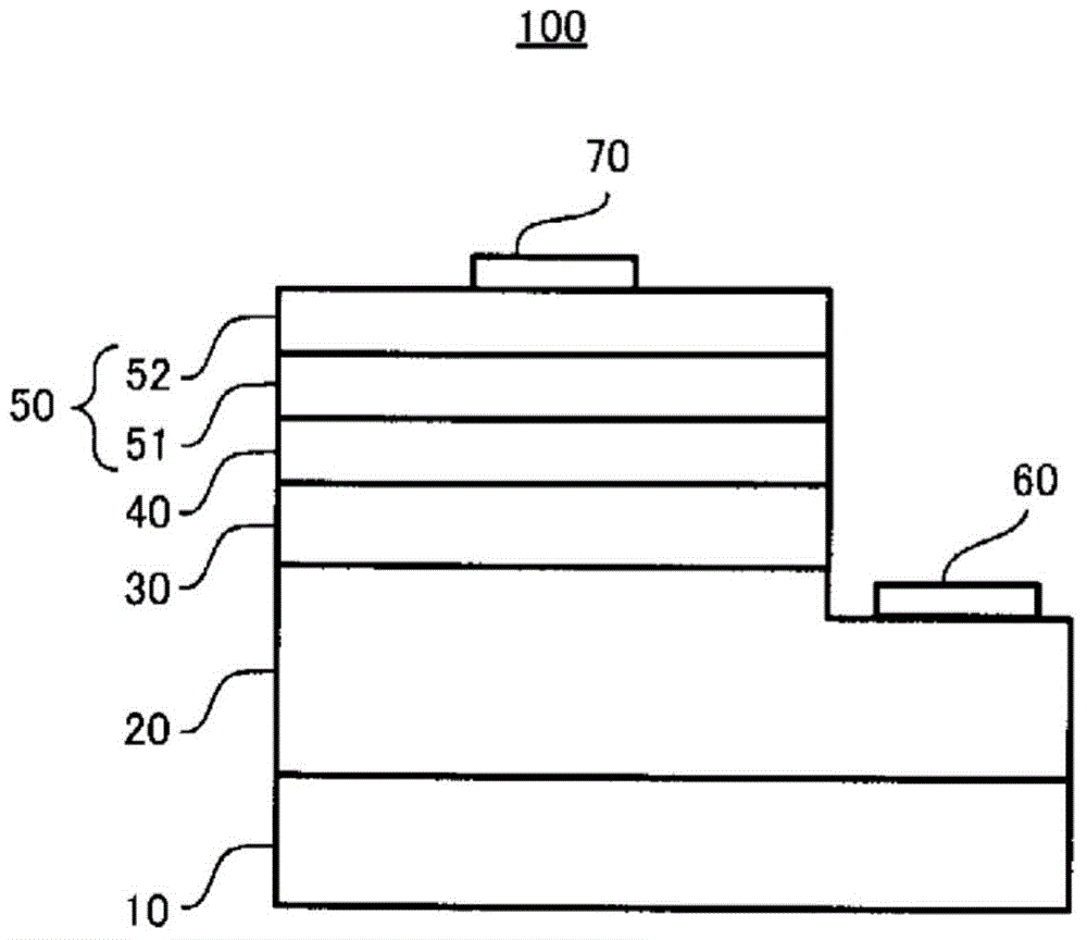
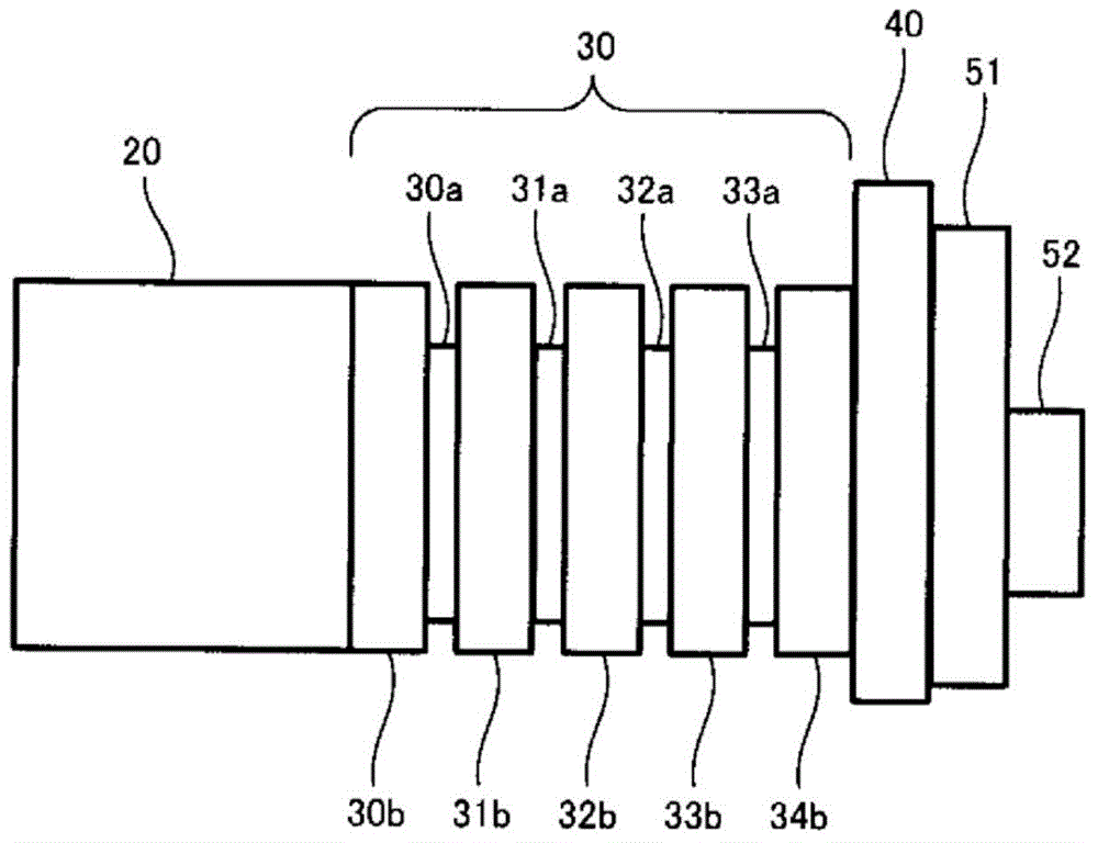
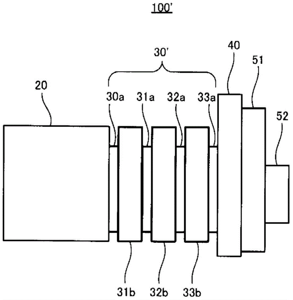
[0109] In the above description of the present invention, the nitride semiconductor light-emitting device 100 in which the active layer 30 has a quantum well structure and the number of the well layers is four is mainly exemplified, but the present invention is not limited to this form. In the nitride semiconductor light-emitting device of the present invention, when the active layer has a quantum well structure, the number of well layers may be one or multiple. The upper limit of the number of well layers is not particularly limited, but is preferably 10 or less from the viewpoint of productivity of nitride semiconductor light-emitting devices. In addition, it is also possible to manufacture a nitride semiconductor light-emitting element in which the active layer has a bulk structure (double heterostructure) instead of a quantum well structure. When the active layer 30 is composed of a monolithic struc...

Embodiment approach (2

[0113] (Other embodiment (2): form having a p-type third layer)

[0114] In the above description of the nitride semiconductor light emitting device of the present invention, the nitride semiconductor light emitting device 100 in which the active layer 30 and the electron blocking layer 40 are in direct contact is mainly exemplified, but the present invention is not limited to this form. A nitride semiconductor light-emitting element in which a p-type third layer is provided between the active layer and the electron blocking layer can also be used. Figure 6 It is a schematic cross-sectional view of a nitride semiconductor light emitting element 200 of such another embodiment. also, Figure 7 for illustration Figure 6 An example of the energy band diagram of the nitride semiconductor light-emitting element 200. exist Figure 6 as well as Figure 7 in, for with Figure 1-5 The same elements as those appearing in the Figure 1-5 The symbols in the same symbols are omitte...

Embodiment approach (3

[0118] (Other embodiment (3): form in which the n-type layer is composed of a plurality of layers)

[0119] In the above description related to the present invention, the nitride semiconductor light-emitting element 100 in which the n-type layer is a single layer, that is, the n-type layer 20 is an n-type first layer having the smallest bandgap in the n-type layer is mainly exemplified. 200, but the present invention is not limited to this form. A nitride semiconductor light-emitting device in the form of an n-type layer composed of a plurality of layers can also be produced. The nitride semiconductor light-emitting device of the present invention in such other embodiments will be described below.


PUM


Abstract

Provided is a nitride semiconductor deep ultraviolet light-emitting element having exceptional light-emitting efficiency. A nitride semiconductor light-emitting element having a light-emission wavelength of 200-300 nm, wherein said element has an n-type layer comprising a single layer or a plurality of layers with differing bandgaps, a p-type layer comprising a single layer or a plurality of layers with differing bandgaps, and an active layer arranged between the n-type layer and the p-type layer. The p-type layer has a p-type first layer having a bandgap that is larger than the bandgap of the n-type first layer having the smallest bandgap within the n-type layer. An electron block layer is provided between the active layer and the p-type first layer, the electron block layer having a bandgap that is larger than the bandgaps of any of the layers forming the active layer and the p-type layer.

Description

technical field [0001] The present invention relates to a novel deep ultraviolet light-emitting element using a nitride semiconductor with a light-emitting wavelength in the range of 200-300nm. Background technique [0002] Currently, a gas light source such as deuterium or mercury is used as a deep ultraviolet light source having an emission wavelength of 300 nm or less. These gas light sources have disadvantages such as short lifetime and large size. In addition, mercury is a substance restricted by the treaty. Therefore, realization of a deep-ultraviolet light-emitting element using a semiconductor that eliminates these inconveniences and is easy to handle has been desired. [0003] However, light-emitting elements using semiconductors have problems of weaker light output and lower luminous efficiency than gas light sources such as deuterium gas lamps and mercury gas lamps. [0004] As the cause of insufficient light output of the semiconductor light-emitting element, ...

Claims


Application Information

Patent Timeline
Patent Type & Authority Applications(China)
IPC IPC(8): H01L33/32H01S5/343
CPCH01L33/04H01L33/32H01S5/2009H01S5/34333H01L33/06H01L33/145H01L33/0025
Inventor 小幡俊之
Owner STANLEY ELECTRIC CO LTD
Why Eureka
Try Eureka