Metal grid transparent conducting film, preparation method thereof and capacitive touch screen

A technology of capacitive touch screen and transparent conductive film, which is applied in the direction of electrical digital data processing, instruments, data processing input/output process, etc., can solve the problems of inability to obtain metal mesh transparent conductive film in mass production, and achieve uniform line width , good visibility effect

Inactive Publication Date: 2015-11-11
ZHANGJIAGANG KANGDE XIN OPTRONICS MATERIAL
View PDF12 Cites 12 Cited by
  • Summary
  • Abstract
  • Description
  • Claims
  • Application Information

AI Technical Summary

Problems solved by technology

[0008] The purpose of this application is to provide a metal grid transparent conductive film, its preparation method and capacitive touch screen to solve the problem that in the prior art, it is impossible to mass-produce a metal grid with a line width of microns or several nanometers and a relatively uniform line width. Problems with transparent conductive film

Method used


Image

  • Metal grid transparent conducting film, preparation method thereof and capacitive touch screen
  • Metal grid transparent conducting film, preparation method thereof and capacitive touch screen
  • Metal grid transparent conducting film, preparation method thereof and capacitive touch screen

Examples


preparation example Construction

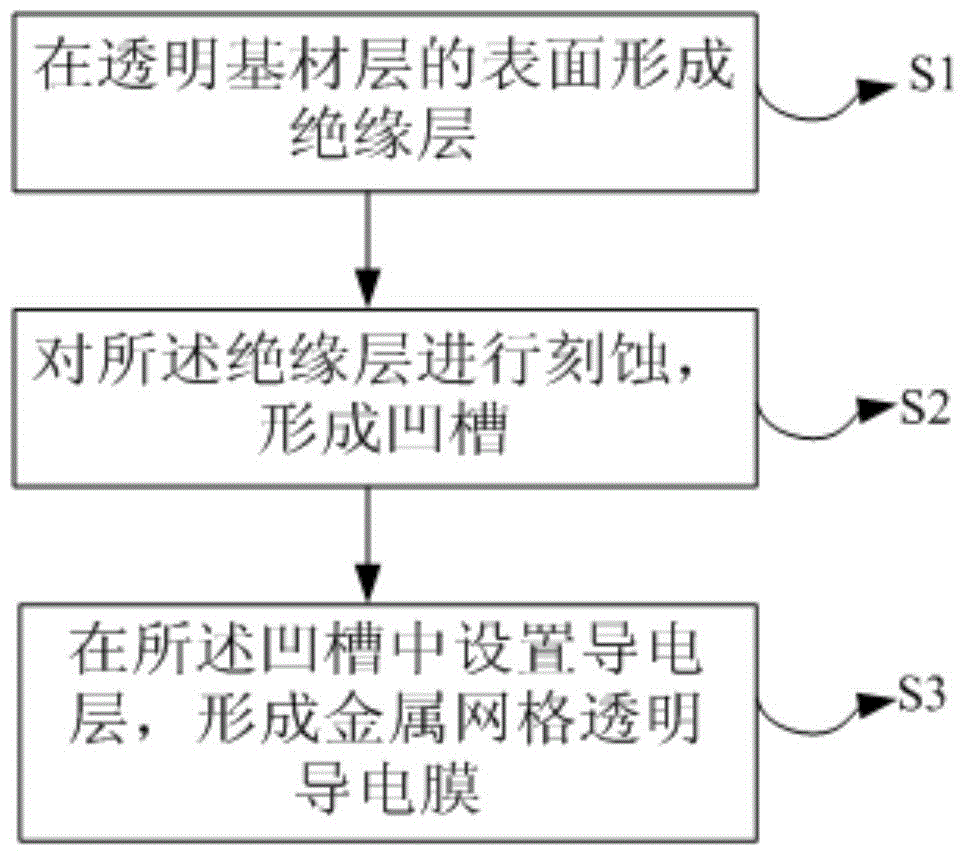
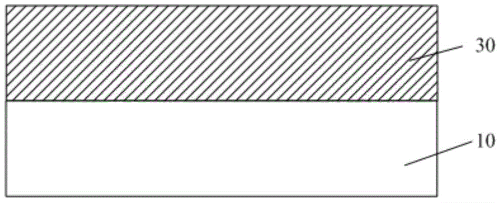
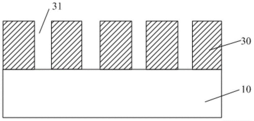
[0035] In a typical implementation of the present application, such as figure 1 As shown, a method for preparing a metal grid transparent conductive film is proposed, the method includes: step S1, forming an insulating layer 30 on the surface of the transparent substrate layer 10, such as figure 2 shown; step S2, for figure 2 The insulating layer 30 in the middle is etched to form a groove 31, such as image 3 shown; and step S3, the conductive layer 50 is set in the above-mentioned groove 31, forming Figure 4b The metal mesh transparent conductive film is shown.

[0036] In this method, an insulating layer 30 is first provided on the surface of the transparent substrate layer 10, and then it is etched to form a groove 31. The material of the insulating layer 30 is generally photosensitive glue, which is more dense than the material of the conductive layer 50. It is easy to form a fine structure, so the line width of the groove 31 formed by etching the insulating layer 3...

Embodiment 1

[0059] First, in Figure 7 The thickness shown is 1.5 μm on the second hardened protective layer 15, and the PCZ001 glue of DIC Company of Japan is wet-coated to obtain an insulating photosensitive glue layer with a dry film thickness of 10 μm. After exposure, the width of the non-hollowed part in the hollowed-out light-shielding plate is 5 μm, the width of the hollowed-out part is 100 μm, and the exposure amount is 800 mJ / cm2, so that the part of the insulating photosensitive glue layer that is not blocked by the light-shielding plate hardens and is shielded from light. The part shielded by the plate was not hardened, and an insulating layer was formed, and the thickness of the hardened part was 10 μm.

[0060] Then, use solvent MIBK (MethylIsobutylKetone, methyl isobutyl ketone) to perform wet etching on the structure of the insulating layer, remove the unhardened insulating photosensitive glue layer, form grooves and dry them.

[0061] Finally, silver paste was coated on t...

Embodiment 2

[0063] First, in Figure 7 The thickness shown is 1.5 μm, and the PCZ001 glue of DIC Company of Japan is set on the second hardened protective layer 15 to obtain an insulating photosensitive glue layer with a dry film thickness of 10 μm. , where the width of the non-hollowed out part in the hollowed-out visor is 5 μm, the width of the hollowed out part is 100 μm, and the exposure amount is 800 mJ / cm 2 , so that the part of the insulating photosensitive glue layer that is not covered by the light-shielding plate is hardened, and the covered part is not hardened, thereby forming an insulating layer, and the thickness of the hardened part is 10 μm.

[0064] Then, the solvent MIBK is used to perform wet etching on the structure forming the insulating layer, remove the unhardened glue, form grooves and dry them.

[0065] Finally, copper paste was coated on the surface of the structure from which the unhardened glue was removed, and after the copper paste was heated and hardened, a...


PUM

PropertyMeasurementUnit
widthaaaaaaaaaa
wavelengthaaaaaaaaaa
thicknessaaaaaaaaaa

Abstract

The invention provides a metal grid transparent conducting film, a preparation method thereof and a capacitive touch screen. The preparation method of the metal grid transparent conducting film includes the steps that S1, insulating layers are formed on the surface of a transparent base material layer; S2, the insulating layers are etched, so that grooves are formed; S3, conducting layers are arranged in the grooves, and accordingly the metal grid transparent conducting film is formed. The metal grid transparent conducting film prepared through the method is even in line width, and the micron grade and even hundreds-of-nanometer grade can be achieved. The preparation method is suitable for mass production of metal grid transparent conducting films, and the yield of the metal grid transparent conducting films can be increased.

Description

technical field [0001] The present application relates to the technical field of transparent conductive films, in particular, to a metal grid transparent conductive film, its preparation method and a capacitive touch screen. Background technique [0002] As an alternative and improved product of ITO (Indium Tin Oxide, tin-doped indium oxide) thin film, the development of metal grid transparent conductive thin film is gradually rising. [0003] There are two methods for preparing metal grid transparent conductive films in the prior art: the first method is to use metal materials such as silver and copper or oxides to obtain easily and cheap conductive layer raw materials, and press them on plastic films such as PET. Formed metal grid pattern, then the raw material of conductive layer is filled in metal grid pattern, forms metal grid transparent conductive film; Laser etching) to form a metal mesh transparent conductive film. [0004] It is difficult for the above two prepar...

Claims


Application Information

Patent Timeline
Patent Type & Authority Applications(China)
IPC IPC(8): G06F3/044
Inventor 张国臻
Owner ZHANGJIAGANG KANGDE XIN OPTRONICS MATERIAL
Why Eureka
Try Eureka