Thin-film structure light-emitting diode (LED) chip based on silver-based metal bonding and preparation method of thin-film structure LED chip

A technology of LED chip and thin film structure, used in semiconductor devices, electrical components, circuits, etc.

Active Publication Date: 2015-11-11
PEKING UNIV +1
View PDF5 Cites 8 Cited by
  • Summary
  • Abstract
  • Description
  • Claims
  • Application Information

AI Technical Summary

Problems solved by technology

[0006] In order to solve the problem of bonding cost and reliability, the invention provides a silver-based metal bonded thin-film

Method used


Image

  • Thin-film structure light-emitting diode (LED) chip based on silver-based metal bonding and preparation method of thin-film structure LED chip
  • Thin-film structure light-emitting diode (LED) chip based on silver-based metal bonding and preparation method of thin-film structure LED chip
  • Thin-film structure light-emitting diode (LED) chip based on silver-based metal bonding and preparation method of thin-film structure LED chip

Examples


Embodiment Construction

[0069] In the following, the present invention will be further described by taking a vertically structured LED chip as an example in conjunction with the accompanying drawings.

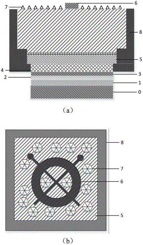
[0070] like figure 1 As shown, the thin-film structure LED chip unit of the vertical structure of this embodiment includes: transfer substrate 0, bonding metal layer 1, transition layer 2, reflective layer 3, p-electrode 4, LED epitaxial layer 5, n-electrode 6, n Surface light cone 7 and passivation layer 8; wherein, on the transfer substrate 0 from bottom to top are bonding metal layer 1, transition layer 2, reflective layer 3, p-electrode 4 and LED epitaxial layer 5; on the LED epitaxial layer N-electrode 6 is formed on a small part of the LED epitaxial layer; n-surface light-emitting cone 7 is formed on the surface of the LED epitaxial layer except for the n-electrode; reflective layer 3 and n-surface light-emitting cone 7 form a light-emitting structure; between LED chip units The sidewalls of th...


PUM


Abstract

The invention discloses a thin-film structure light-emitting diode (LED) chip based on silver-based metal bonding and a preparation method of the thin-film structure LED chip. AgCuIn alloy is adopted as a bonding metal layer, so that the bonding temperature is reduced and the retention time is shortened; AgCuIn bonding can be finished at relatively low bonding temperature and bonding pressure; the bonding time is shortened; reduction of the injuries to the photoelectric property of an LED epitaxial layer in the bonding process is facilitated; by a bonding metal layer of the AgCuIn alloy, the cavity phenomenon in the bonding process is removed; stress release of the LED epitaxial layer is facilitated; the AgCuIn bonding is high in mechanical property and has good conductivity and heat-conducting property; prolonging of the service life of the LED chip is facilitated; with the AgCuIn as bonding metal, the manufacturing cost of the vertical structure LED chip is greatly reduced; and marketing development of the vertical structure LED chip is facilitated.

Description

technical field [0001] The invention relates to a thin-film structure LED chip, in particular to a thin-film structure LED chip based on silver-based metal bonding and a preparation method thereof. Background technique [0002] The GaN-based power thin-film structure light-emitting diode LED based on laser lift-off and bonding technology has a very broad application prospect in the field of high-power lighting. The key step of this scheme is to bond the GaN epitaxial layer grown on sapphire to a conductive and thermally conductive transfer substrate such as Si or Cu after preparing the p-electrode and other p-plane structures, and then use laser lift-off technology to remove it as the growth substrate. sapphire, and roughen the surface of the exposed N-polar GaN surface, and then prepare the n-electrode. The bonding technology needs to achieve high bond strength to ensure the yield, and it needs to have good electrical and thermal conductivity to reduce the resistance and i...

Claims


Application Information

Patent Timeline
IPC IPC(8): H01L33/48
CPCH01L33/48
Inventor 陈志忠马健陈景春姜爽焦倩倩李俊泽蒋盛翔李诚诚康香宁秦志新张国义
Owner PEKING UNIV
Why Eureka
Try Eureka