Image sensor chip packaging method

A sensor chip and packaging method technology, which is applied in the direction of radiation control devices, electrical components, electric solid devices, etc., can solve the problems of increasing the thickness of the packaging body and complicated manufacturing process, and achieve the advantages of reduced packaging process, simple packaging process and good protection Effect

Inactive Publication Date: 2015-11-18
HUATIAN TECH KUNSHAN ELECTRONICS
View PDF5 Cites 18 Cited by
  • Summary
  • Abstract
  • Description
  • Claims
  • Application Information

AI Technical Summary

Problems solved by technology

This structure will increase the thickness of the package, and it is necessary to make a cofferdam structure, which makes the manufacturing process complicated

Method used


Image

  • Image sensor chip packaging method
  • Image sensor chip packaging method
  • Image sensor chip packaging method

Examples


Embodiment 1

[0042] A method for packaging an image sensing chip, performed in the following steps:

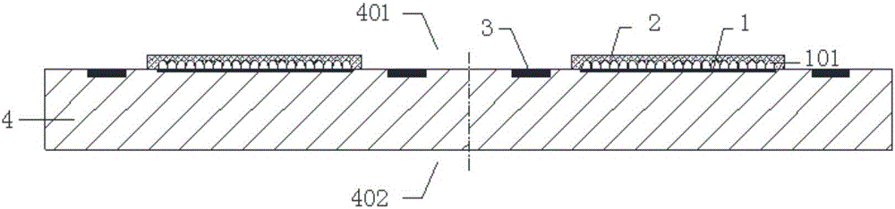
[0043] a. see Figure 1a , provide a wafer 4 with some image sensing chips, the front side 401 of the wafer is the functional surface of the image sensing chip, the back side 402 of the wafer is the lower surface of the base of the image sensing chip, the function of each image sensing chip The surface has a photosensitive area 1 and several welding pads 3 located around the photosensitive area, and the photosensitive area is coated with a dielectric film 2 with insulation, high light transmission, resistance to wiping and erosion of liquid medicine; There is a cutting line between the image sensor chips for cutting and separating into single chip units. The center position of the cutting line is as follows: Figure 1a Shown by the dotted line.

[0044] In this embodiment, the dielectric film is a cube structure parallel to the wafer surface, such as Figure 1a shown. In other embodiments...

Embodiment 2

[0057]A method for packaging an image sensing chip, performed in the following steps:

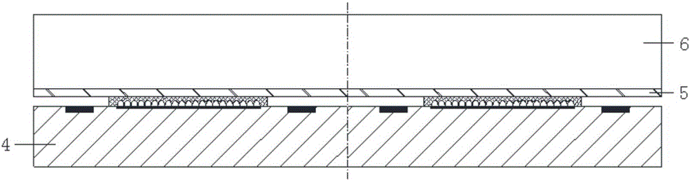
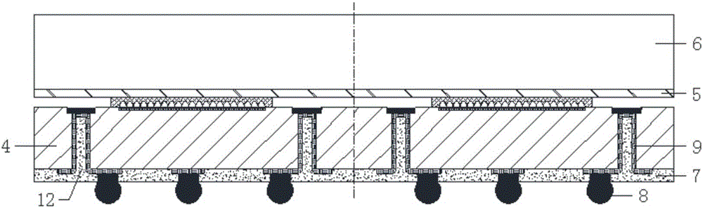
[0058] a. see Figure 2a , provide a wafer 4 with some image sensing chips, the front side 401 of the wafer is the functional surface of the image sensing chip, the back side 402 of the wafer is the lower surface of the base of the image sensing chip, the function of each image sensing chip The surface has a photosensitive area 1 and several welding pads 3 located around the photosensitive area, and the photosensitive area is covered with a dielectric film 2 with insulation, high light transmission, resistance to wiping and corrosion by liquid medicine; There are dicing lines between the image sensor chips; and the welding pads on the front of the chip are partially exposed, and metal bumps 13 are plated on the welding pads on the front of the chip;

[0059] b. providing a carrier 6 having a first surface and a second surface opposite thereto;

[0060] c. see Figure 2b , setting a bondi...


PUM


Abstract

The invention provides an image sensor chip packaging method. The method comprises the steps of covering a photosensitive zone of an image sensor chip with a layer of dielectric film which is characterized by high light transmitting performance, insulation, drug liquid resistance and wiping resistance; bonding a carrier plate for the dielectric film of the chip directly and temporarily, the carrier plate serving as the support for a back manufacture procedure of the chip; then performing the back manufacture procedure of the chip; finally removing the bonding after the back manufacture procedure is finished and obtaining single image sensor chip package bodies through cutting. The dielectric film covering the photosensitive zone of the chip has the characteristics of high light transmitting performance, insulation, drug liquid resistance and wiping resistance, so that scratching or drug liquid corrosion damage can be prevented, the photosensitive zone of the chip can be better protected and the imaging effect can be guaranteed. The packaging process is simple; the manufacture procedures are reduced; the thickness of the chip package bodies is reduced.

Description

technical field [0001] The invention relates to a packaging method for an image sensing chip, in particular to a packaging method for an image sensing chip without cofferdams. Background technique [0002] During the packaging process of the image sensor chip, its photosensitive area needs to be isolated to prevent the photosensitive area from being polluted by micro particles. The prior art process for protecting the photosensitive area is to bond a transparent cover plate with a cofferdam on the image sensor chip, wherein the cofferdam surrounds the photosensitive area so that the photosensitive area forms a sealed space. This structure will increase the thickness of the package body, and the cofferdam structure needs to be fabricated, which complicates the manufacturing process. It is necessary to find a method that can not only protect the photosensitive area from pollution, but also reduce the thickness of the packaging body and reduce the packaging process. Contents...

Claims


Application Information

Patent Timeline
IPC IPC(8): H01L21/50H01L21/56H01L27/146H01L23/29
CPCH01L21/50H01L21/56H01L23/29H01L27/146H01L27/14683H01L2224/11
Inventor 肖智轶黄小花万里兮王晔晔刘磊翟玲玲徐军
Owner HUATIAN TECH KUNSHAN ELECTRONICS
Why Eureka
Try Eureka