TFT substrate manufacturing method and TFT substrate

A manufacturing method and substrate technology, which are used in semiconductor/solid-state device manufacturing, semiconductor devices, electrical components, etc., can solve the problems of poor uniformity, poor on-current and sub-threshold slope, and poor driving ability of low-temperature polysilicon thin-film transistors. Achieve the effect of reducing channel photo-leakage, reducing sub-threshold slope, and good grain uniformity

Inactive Publication Date: 2015-11-18
TCL CHINA STAR OPTOELECTRONICS TECH CO LTD
View PDF9 Cites 19 Cited by
  • Summary
  • Abstract
  • Description
  • Claims
  • Application Information

AI Technical Summary

Problems solved by technology

The current situation is that the low-temperature polysilicon thin-film transistors produced by the ELA method have poor uniformity and high cost. Although the SPC method can reduce costs and improve uniformity, its on-current and sub-threshold slope are not as good as the ELA method. The low-temperature polysilicon thin film transistor produced has a large off current, so the driving ability is poor

Method used


Image

  • TFT substrate manufacturing method and TFT substrate
  • TFT substrate manufacturing method and TFT substrate
  • TFT substrate manufacturing method and TFT substrate

Examples


Embodiment Construction

[0041] In order to further illustrate the technical means adopted by the present invention and its effects, the following describes in detail in conjunction with preferred embodiments of the present invention and accompanying drawings.

[0042] The present invention at first provides a kind of manufacturing method of TFT substrate, comprises the following steps:

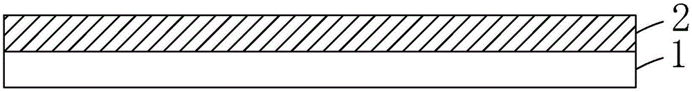
[0043] Step 1, such as figure 1 As shown, a substrate 1 is provided, and after the substrate 1 is cleaned and prebaked, a buffer layer 2 is deposited on the substrate 1 .

[0044] Specifically, the substrate 1 may be a glass substrate.

[0045] Specifically, the buffer layer 2 may be a single-layer structure composed of silicon nitride, a single-layer structure composed of silicon oxide, or a double-layer structure composed of a silicon nitride layer and a silicon oxide layer. Preferably, the buffer layer 2 has a thickness of 500-2000A.

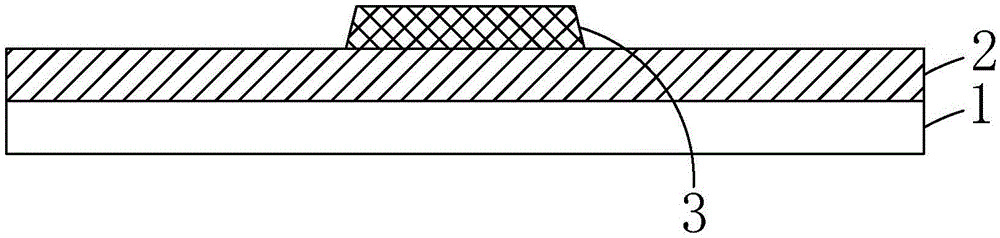
[0046] Step 2, such as figure 2 As shown, a first metal layer is deposited...


PUM


Abstract

The invention provides a TFT substrate manufacturing method and a TFT substrate. The method employs the SPC (Solid Phase Crystallization) technology to prepare an LTPS (Low Temperature Poly-Silicon) layer, and can reduce costs and form crystalline grains with better uniformity compared with the excimer laser crystallization technology; meanwhile, a bigrid structure is introduced, thereby enhancing the control of grids to channels, increasing the on state current of a film transistor, reducing off state current, inhibiting warping effects, reducing a threshold voltage and a subthreshold gradient, and improving the driving capability of the film transistor; besides, top grids can cover light, and reduce channel photoinduced electric leakage. The invention provides the TFT substrate, the LTPS layer of which is prepared through the SPC technology, and the TFT is low in production costs; in addition, the TFT substrate is provided with the bigrid structure, allowing the film transistor to have better electric property and strong driving capability, and not easy to generate channel photoinduced electric leakage.

Description

technical field [0001] The invention relates to the field of display technology, in particular to a method for manufacturing a TFT substrate and the prepared TFT substrate. Background technique [0002] With the development of flat panel displays, the demand for panels with high resolution and low energy consumption is constantly being raised. Low-temperature polysilicon (LowTemperaturePoly-Silicon, LTPS) has been valued by the industry in liquid crystal display (LiquidCrystalDisplay, LCD) and organic light-emitting diode display (OrganicLightEmittingDiode, OLED) technology due to its high electron mobility. Important materials for cost-effective full-color flat-panel displays. For flat panel displays, low-temperature polysilicon materials have the advantages of high resolution, fast response, high brightness, high aperture ratio, and low energy consumption, and low-temperature polysilicon can be produced at low temperatures and can be used to make C-MOS (Complementary Meta...

Claims


Application Information

Patent Timeline
Patent Type & Authority Applications(China)
IPC IPC(8): H01L27/12H01L29/66H01L29/423H01L29/786
CPCH01L27/1222H01L27/1237H01L27/1285H01L29/42384H01L29/66765H01L29/78648H01L21/02532H01L21/02592H01L21/02667H01L21/26513H01L29/78618H01L29/78633H01L29/78678
Inventor 周星宇吴元均
Owner TCL CHINA STAR OPTOELECTRONICS TECH CO LTD
Why Eureka
Try Eureka