Printed circuit board with blind holes and processing method of printed circuit board

A technology for printed circuit boards and processing methods, applied in printed circuits, printed circuits, printed circuit manufacturing, etc., can solve the problems of slag residue, long laser time, laser penetration, etc., to achieve diversity and no slag residue. Effect

Inactive Publication Date: 2015-11-18
GULTECH WUXI ELECTRONICS CO LTD
View PDF6 Cites 3 Cited by
  • Summary
  • Abstract
  • Description
  • Claims
  • Application Information

AI Technical Summary

Problems solved by technology

[0002] With the rapid development of electronic products, many special products correspond to special needs. The traditional blind hole design is difficult to meet some special needs, such as: buried components and acoustic cavity requirements. If the traditional blind hole laser method is used to make blind holes , the general diameter is 75~150um, and the depth is 30~100um. If you need to make a large blind hole or a deeper blind hole, you need to spend longer laser time and greater laser energy to work, which will cause laser shooting. Problems such as wear, glue residue, and abnormal shape of the hole cannot meet the customer's product function and reliability requirements.

Method used


Image

  • Printed circuit board with blind holes and processing method of printed circuit board
  • Printed circuit board with blind holes and processing method of printed circuit board
  • Printed circuit board with blind holes and processing method of printed circuit board

Examples


Embodiment 1

[0027] A method for processing a printed circuit board with blind holes comprises the following steps:

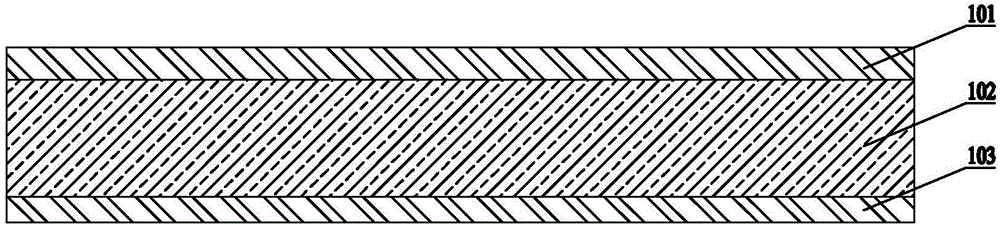
[0028] a. Take the semi-finished printed circuit board. The semi-finished printed circuit board has an upper copper foil layer 101, a base material layer 102 and a lower copper foil layer 103. The upper copper foil layer 101 is arranged on the upper surface of the base material layer 102, and the lower copper foil layer 103 is arranged on the lower surface of the substrate layer 102, the thickness of the upper copper foil layer 101 is 12 μm, the thickness of the substrate layer 102 is 0.05 mm, the material of the substrate layer 102 is FR4, and the thickness of the lower copper foil layer 103 is 12 μm;

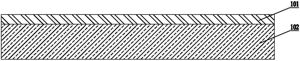
[0029] b. Etching off the copper foil layer 103 by using an etching solution and adopting a conventional etching process, the etching solution is a mixed solution mainly containing copper chloride, hydrochloric acid and hypochlorous acid;

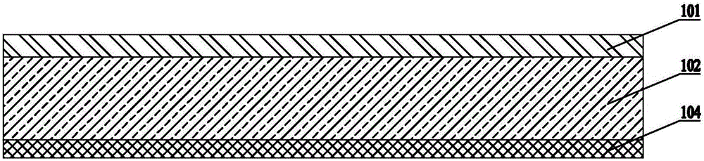
[0030] c. Heating the epoxy resin...

Embodiment 2

[0035] A method for processing a printed circuit board with blind holes comprises the following steps:

[0036] a. Take the semi-finished printed circuit board. The semi-finished printed circuit board has an upper copper foil layer 101, a base material layer 102 and a lower copper foil layer 103. The upper copper foil layer 101 is arranged on the upper surface of the base material layer 102, and the lower copper foil layer 103 is arranged on the lower surface of the substrate layer 102, the thickness of the upper copper foil layer 101 is 105 μm, the thickness of the substrate layer 102 is 3 mm, the material of the substrate layer 102 is FR4, and the thickness of the lower copper foil layer 103 is 105 μm;

[0037] b. Etching off the copper foil layer 103 by using an etching solution and adopting a conventional etching process, the etching solution is a mixed solution mainly containing copper chloride, hydrochloric acid and hypochlorous acid;

[0038] c. Heating the epoxy resin ...

Embodiment 3

[0043] A method for processing a printed circuit board with blind holes comprises the following steps:

[0044] a. Take the semi-finished printed circuit board. The semi-finished printed circuit board has an upper copper foil layer 101, a base material layer 102 and a lower copper foil layer 103. The upper copper foil layer 101 is arranged on the upper surface of the base material layer 102, and the lower copper foil layer 103 is arranged on the lower surface of the substrate layer 102, the thickness of the upper copper foil layer 101 is 50 μm, the thickness of the substrate layer 102 is 1.5 mm, the material of the substrate layer 102 is FR4, and the thickness of the lower copper foil layer 103 is 50 μm;

[0045] b. Etching off the copper foil layer 103 by using an etching solution and adopting a conventional etching process, the etching solution is a mixed solution mainly containing copper chloride, hydrochloric acid and hypochlorous acid;

[0046] c. Heating the epoxy resin ...


PUM


Abstract

The invention discloses a printed circuit board with blind holes and a processing method of the printed circuit board. The printed circuit board comprises an upper copper foil layer, a base material layer, an epoxy resin glue film layer and a copper foil layer for foiling, wherein the upper copper foil layer is arranged on the upper surface of the base material layer; the epoxy resin glue film layer is arranged on the lower surface of the base material layer; the copper foil layer for foiling is arranged on the lower surface of the epoxy resin glue film layer; and blind holes are formed in the upper copper foil layer, the base material layer and the epoxy resin glue film layer. According to the printed circuit board, the diameters and the depths of the blind holes can be arbitrarily combined; the diameters can be realized by selecting the size of a drill pin; the depths can be realized by selecting printed circuit substrates with different thicknesses; the printed circuit board is free of a glue residue, upright in hole pattern, simple in design and easy to process; and the design of the product has large extension, so that the functional diversity of the product can be realized.

Description

technical field [0001] The invention discloses a printed circuit board with blind holes, and also discloses a processing method for the printed circuit board with blind holes. Background technique [0002] With the rapid development of electronic products, many special products correspond to special needs. The traditional blind hole design is difficult to meet some special needs, such as: buried components and acoustic cavity requirements. If the traditional blind hole laser method is used to make blind holes , the general diameter is 75~150um, and the depth is 30~100um. If you need to make a large blind hole or a deeper blind hole, you need to spend longer laser time and greater laser energy to work, which will cause laser shooting. Problems such as wear, slag residue, and abnormal hole shape cannot meet the customer's product function and reliability needs. Contents of the invention [0003] The object of the present invention is to overcome the disadvantages of the pri...

Claims


Application Information

Patent Timeline
Patent Type & Authority Applications(China)
IPC IPC(8): H05K1/11H05K3/40
CPCH05K1/115H05K3/4038H05K2201/09509
Inventor 金小健
Owner GULTECH WUXI ELECTRONICS CO LTD
Why Eureka
Try Eureka