

Copper alloy for electrical and electronic equipment, copper alloy thin sheet for electrical and electronic equipment, and conductive component and terminal for electrical and electronic equipment
A technology for electrical and electronic components, applied in the fields of copper alloys for electrical and electronic equipment, copper alloy sheets for electrical and electronic equipment, conductive components and terminals for electrical and electronic equipment, which can solve the problem of increased weight and the inability to achieve stress relaxation resistance of copper alloys Sufficient and reliable improvement of copper alloys, failure to achieve stress relaxation resistance characteristics of copper alloys, etc.
- Summary
- Abstract
- Description
- Claims
- Application Information
AI Technical Summary
Problems solved by technology
Method used
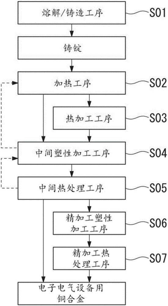
Image

Examples
Embodiment
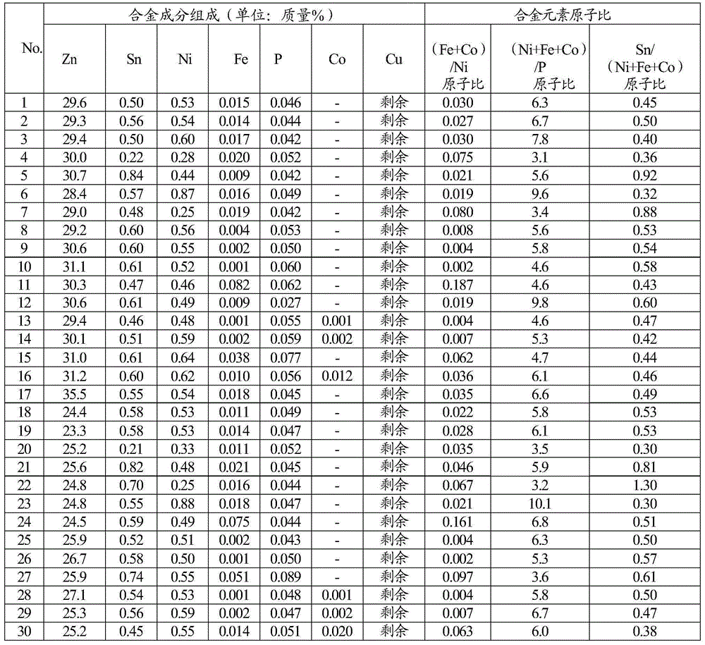
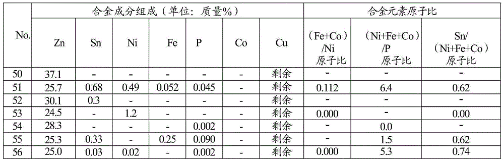
[0145] Hereinafter, the results of confirmation experiments conducted to confirm the effects of the present invention are shown together with comparative examples as examples of the present invention. In addition, the following examples are examples for illustrating the effects of the present invention, and the structures, processes, and conditions described in the examples do not limit the technical scope of the present invention.
[0146] First, a raw material composed of a Cu-40% Zn master alloy and oxygen-free copper (ASTMB152C10100) with a purity of 99.99% by mass or higher was prepared, which was placed in a high-purity graphite crucible, and the 2 Melt in an electric furnace under a gas atmosphere. Various additive elements were added to the copper alloy melt, the alloy melt having the composition shown in Tables 1 and 2 was melted, and poured into a mold to produce an ingot. In addition, the size of the ingot was about 25 mm in thickness x about 50 mm in width x about...
PUM
 Abstract
Description
Claims
Application Information