Copper alloys for electrical and electronic equipment, copper alloy sheets for electrical and electronic equipment, conductive components and terminals for electrical and electronic equipment

A technology for electrical and electronic components, applied in the fields of copper alloys for electrical and electronic equipment, copper alloy sheets for electrical and electronic equipment, conductive components and terminals for electrical and electronic equipment, and can solve the problems of improving stress relaxation resistance, rising material costs, contact It can achieve the effects of sufficiently excellent stress relaxation resistance, reliable stress relaxation resistance, and excellent bending processability without problems such as defects.

Active Publication Date: 2018-10-26
MITSUBISHI MATERIALS CORP +1
View PDF4 Cites 0 Cited by
  • Summary
  • Abstract
  • Description
  • Claims
  • Application Information

AI Technical Summary

Problems solved by technology

[0016] However, in Patent Documents 1 and 2, only the individual contents of Ni, Fe, and P are considered, and it is not always possible to reliably and sufficiently improve the stress relaxation resistance simply by adjusting these individual contents.
[0017] In addition, although Patent Document 3 discloses adjusting the Ni / Sn ratio, the relationship between the P compound and the stress relaxation resistance is not considered at all, and the improvement of the stress relaxation resistance cannot be sufficiently and reliably achieved.
[0018] In addition, in Patent Document 4, sufficient improvement in stress relaxation resistance cannot be achieved only by adjusting the total amount of Fe, Ni, and P and the atomic ratio of (Fe+Ni) / P.
[0019] As described above, conventionally proposed methods cannot sufficiently improve the stress relaxation resistance of Cu-Zn-Sn alloys
Therefore, in the connector with the above-mentioned structure, the residual stress relaxes over time or in a high-temperature environment, so that the contact pressure with the conductive member on the opposite side cannot be maintained, and there is a problem that defects such as poor contact are likely to occur at an early stage.
In order to avoid this problem, in the past, the wall thickness of the material had to be increased, resulting in an increase in material cost and weight

Method used


Image

  • Copper alloys for electrical and electronic equipment, copper alloy sheets for electrical and electronic equipment, conductive components and terminals for electrical and electronic equipment
  • Copper alloys for electrical and electronic equipment, copper alloy sheets for electrical and electronic equipment, conductive components and terminals for electrical and electronic equipment
  • Copper alloys for electrical and electronic equipment, copper alloy sheets for electrical and electronic equipment, conductive components and terminals for electrical and electronic equipment

Examples


Embodiment

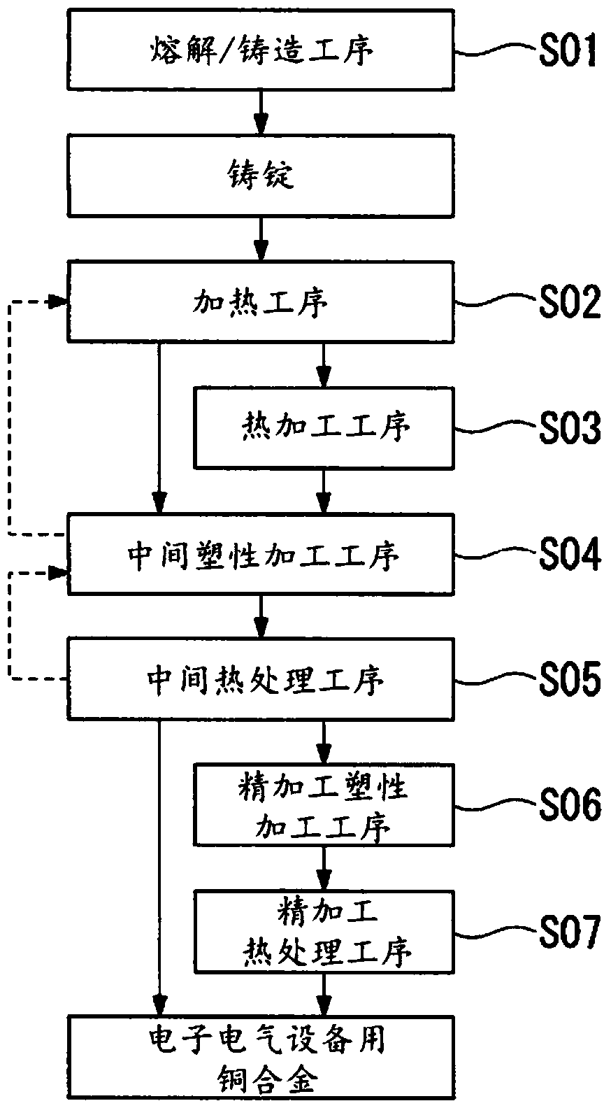
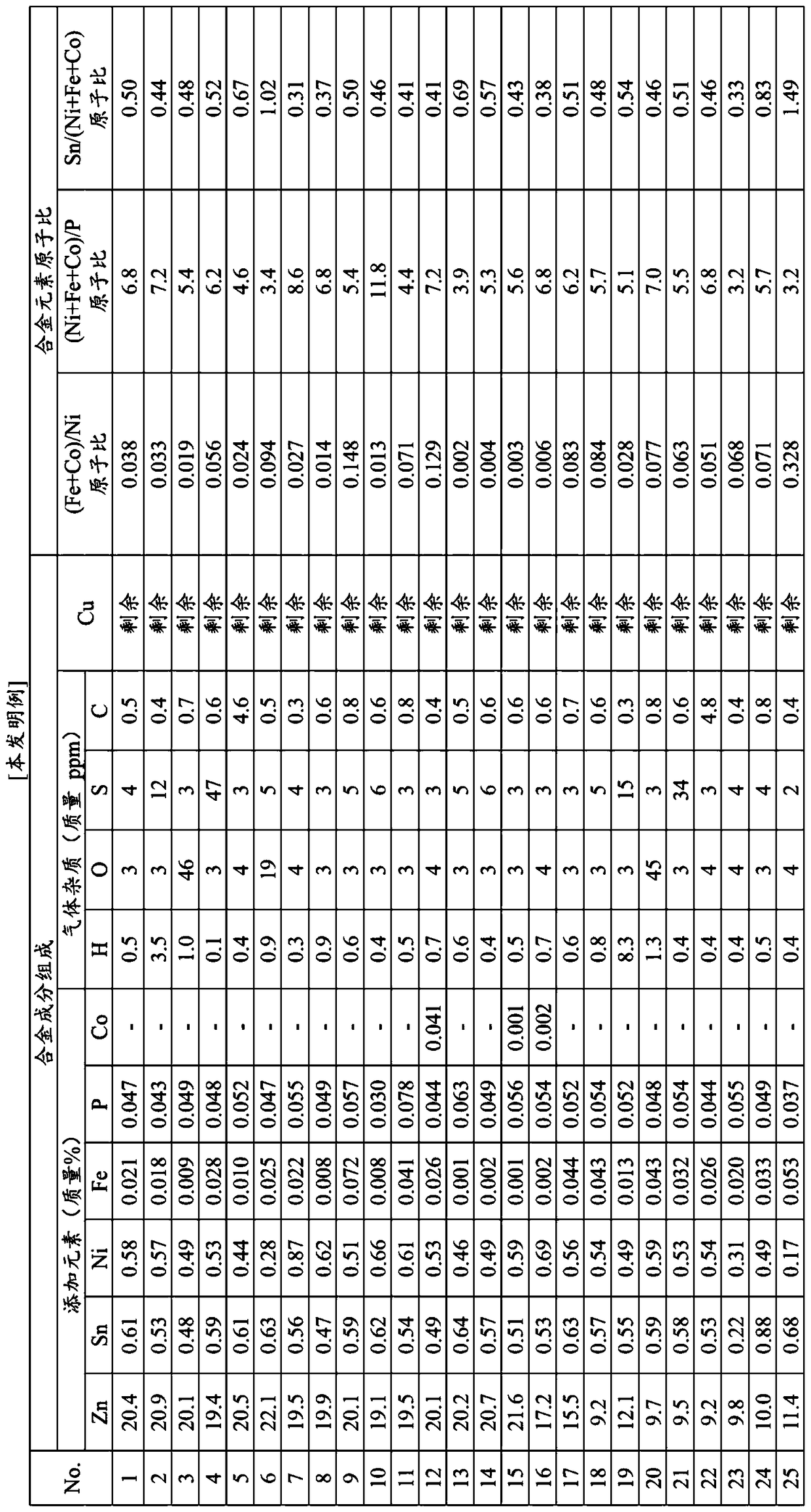
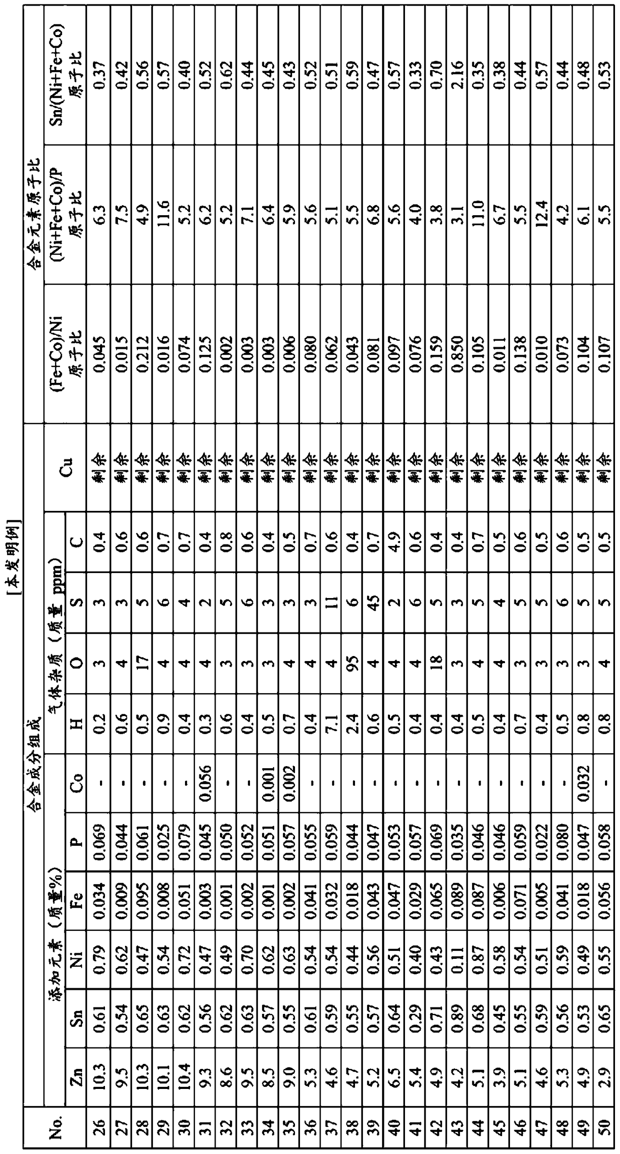
[0144] Hereinafter, the results of confirmation experiments conducted to confirm the effects of the present invention are shown together with comparative examples as examples of the present invention. In addition, the following examples are examples for illustrating the effects of the present invention, and the configurations, processes, and conditions described in the examples do not limit the technical scope of the present invention.

[0145] Prepare a Cu-40% Zn master alloy with an H content of 0.5 ppm or less, an O content of 5 ppm or less, an S content of 5 ppm or less, and a C content of 1 ppm or less. The H content is 1 ppm or less, the O content is 1.5 ppm or less, and the S content is Oxygen-free copper (ASTM B152C10100) with a purity of 99.99 mass% or more (ASTM B152C10100) with a C content of 5ppm or less and a C content of 1ppm or less is used as a raw material. Use a high-frequency melting furnace to melt. When various elements are added to the copper alloy melt an...


PUM

PropertyMeasurementUnit
yield strengthaaaaaaaaaa
thicknessaaaaaaaaaa

Abstract

The present invention relates to a copper alloy for electrical and electronic equipment, a copper alloy sheet for electrical and electronic equipment, a conductive element and a terminal for electrical and electronic equipment. Zn from 0.10 mass % to 0.90 mass % Sn, 0.05 mass % to less than 1.00 mass % Ni, 0.001 mass % to less than 0.100 mass % Fe, 0.005 mass % to 0.100 mass % P , the rest is composed of Cu and unavoidable impurities, and in terms of atomic ratio, it satisfies 0.002≤Fe / Ni<1.500, 3.0<(Ni+Fe) / P<100.0, 0.10<Sn / (Ni+Fe)<5.0 , and the H content is 10 mass ppm or less, the O content is 100 mass ppm or less, the S content is 50 mass ppm or less, and the C content is 10 mass ppm or less.

Description

technical field [0001] The present invention relates to a Cu-Zn-Sn series copper alloy for electrical and electronic equipment used as a conductive element for electrical and electronic equipment such as a connector of a semiconductor device, other terminals, or a movable conductive sheet of an electromagnetic relay, or a lead frame. The copper alloy thin plate for electronic and electrical equipment of the copper alloy for electronic and electrical equipment, a conductive element and a terminal for electronic and electrical equipment. [0002] This application claims priority based on Patent Application No. 2012-282680 filed in Japan on December 26, 2012 and Patent Application No. 2013-252330 filed in Japan on December 5, 2013, and the contents thereof are incorporated herein by reference. middle. Background technique [0003] Cu—Zn alloys have conventionally been widely used as raw materials for the above-mentioned electric and electronic conductive elements from the view...

Claims


Application Information

Patent Timeline
Patent Type & Authority Patents(China)
IPC IPC(8): C22C9/04C22F1/08H01B1/02H01B5/02C22F1/00
CPCC22C9/04C22F1/002C22F1/02C22F1/08H01B1/026Y10T428/12Y10T428/12715B32B15/01
Inventor 牧一诚森广行山下大树
Owner MITSUBISHI MATERIALS CORP
Why Eureka
Try Eureka