
EUV (extreme UV) lithographic apparatus and exposure method therefor

A lithography and exposure bit technology, applied in the field of lithography, can solve the problems of difficult mask heat dissipation, time-consuming, affecting productivity, etc., and achieve the effects of reducing exposure feedback adjustment time, avoiding image quality damage, and improving productivity.

Active Publication Date: 2015-11-25
SHANGHAI MICRO ELECTRONICS EQUIP (GRP) CO LTD
View PDF8 Cites 2 Cited by
  • Summary
  • Abstract
  • Description
  • Claims
  • Application Information

AI Technical Summary

Problems solved by technology

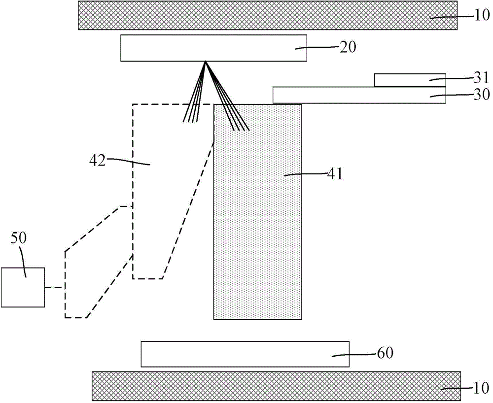
[0007] 1. During the continuous exposure of multiple batches of EUV lithography, before the exposure of the first silicon wafer in each batch, it is necessary to exchange the mask at the exchange position, measure the mask surface at the measurement position, and then measure the mask surface at the exposure position. Exposure, especially when performing a double exposure or multiple exposure process, the switching of each mask and the measurement of the subsequent operations need to be performed serially, thus affecting the yield
[0008] 2. In the EUV high-vacuum environment, it is more difficult to dissipate heat from the mask. When a mask is continuously exposed, the mask absorbing layer is deformed due to heat, which affects the imaging quality. It is necessary to wait for cooling treatment to affect the yield
[0009] 3. The EUV lithography system is particularly sensitive to the environment. When it is necessary to use a calibration mask to calibrate the system, mask replacement and surface measurement take time and affect productivity

Method used


Image

  • EUV (extreme UV) lithographic apparatus and exposure method therefor
  • EUV (extreme UV) lithographic apparatus and exposure method therefor
  • EUV (extreme UV) lithographic apparatus and exposure method therefor

Examples


Embodiment 1

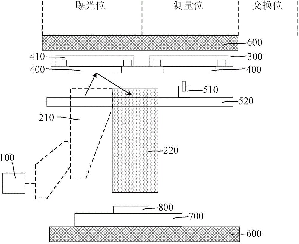
[0045] Please refer to figure 2 In this embodiment, an EUV lithography apparatus is proposed, which includes: EUV light source 100, illumination system 210, projection system 220, workpiece stage 700, mask stage 300, and mask surface type combined measurement system; The EUV lithography apparatus is divided into an exposure position and a measurement position. The projection system 220 and the workpiece table 700 are located in the exposure position, and the mask surface type combined measurement system is located in the measurement position; the mask table 300 carries a plurality of reflective The mask 400, the light emitted by the EUV light source 100 passes through the illumination system 210, the reflective mask 400 on the mask stage, and the projection system 220 to irradiate onto the workpiece stage 700 (as shown by the arrow in the figure). The combined mask surface measurement system measures the surface and position of the reflective mask at the measurement position.

...

Embodiment 2

[0064] Please refer to Figure 5 In this embodiment, an EUV lithography apparatus is proposed. On the basis of the first embodiment, two combined area sensors 510 are provided, which are located at the first measurement position and the second measurement position, respectively. The measurement position and the second measurement position are respectively located on both sides of the exposure position. The mask stage 300 carries three reflective masks 400, and the reflective mask 400 is carried by the mask stage 410 and the mask stage. 300 is connected, one reflective mask 400 is located at the exposure position, and the other two reflective masks 400 are located at the first measurement position and the second measurement position respectively, and are combined with the two combinations of the first measurement position and the second measurement position The area sensor 510 faces each other.

[0065] The EUV lithography apparatus and EUV lithography exposure method proposed in ...

Embodiment 3

[0068] Please refer to Image 6 In this embodiment, an EUV lithography apparatus is proposed, which includes two combined area sensors 510 and two measurement positions. The two measurement positions are the first measurement position and the second measurement position, respectively Both sides of the bit.

[0069] However, in this embodiment, the mask table 300 only carries two reflective masks 400, and the mask table 300 can follow Image 6 The arrow in the middle moves horizontally, so that the two reflective masks 400 can be switched between the first measurement position, the exposure position, and the second measurement position.

[0070] The rest of the device and exposure method are the same as the first embodiment, and will not be repeated here. For details, please refer to the first embodiment.

[0071] In summary, in the EUV lithography apparatus and its exposure method provided by the embodiments of the present invention, since the mask table carries a plurality of refl...


PUM


Abstract

An EUV photoetching device and an exposure method therefor. A mask table (300) of the device bears a plurality of reflection type masks (400a, 400b), wherein while one reflection type mask (400a) at an exposure position conducts exposure, the other reflection type mask (400b) at a measurement position can conduct facial forming and position measurement simultaneously. When a plurality of batches of silicon chips are exposed, the time for facial forming and position measurement can be saved, thereby improving the productivity. The mask table (300) can also bear a plurality of identical reflection type masks, and silicon chips are exposed by using a manner of switching masks alternately, so that by means of continuously switching the reflection type masks, the occurrence of the situation where the image quality is impaired, which is caused by the thermal deformation of the reflection type masks after being exposed for a period of time, due to the fact that heat dissipation in a high vacuum environment is difficult can be avoided.

Description

Technical field [0001] The invention relates to the field of lithography, and in particular to an EUV lithography device and an exposure method thereof. Background technique [0002] Projection exposure device is a device for projecting and exposing the circuit pattern on the mask through a projection optical system, and can project the circuit pattern on the silicon wafer for manufacturing integrated circuits at a certain magnification or reduction ratio. The development of integrated circuits follows "Moore's Law". With the rapid development of IC manufacturing technology, IC integration is gradually increasing, and the wavelength of light used by projection exposure devices is also gradually decreasing. The current mainstream photolithography technology uses 193nm (DeepUV; DUV) wavelength Laser. Driven by technological innovations such as immersion technology, double exposure and multiple exposure, it is gradually approaching the lithography limit that DUV wavelengths can rea...

Claims


Application Information

Patent Timeline
IPC IPC(8): G03F7/20
CPCG03F7/20H01L21/00
Inventor 郑乐平许琦欣王帆吴飞
Owner SHANGHAI MICRO ELECTRONICS EQUIP (GRP) CO LTD
Learn More