Formation method of semiconductor structure

一种半导体、栅极结构的技术,应用在半导体结构的形成领域,能够解决抬高源/漏区缺陷等问题

Active Publication Date: 2015-11-25
SEMICON MFG INT (SHANGHAI) CORP
View PDF3 Cites 6 Cited by
  • Summary
  • Abstract
  • Description
  • Claims
  • Application Information

AI Technical Summary

Problems solved by technology

[0007] However, there are still defects in the raised source / drain regions formed by the prior art

Method used


Image

  • Formation method of semiconductor structure
  • Formation method of semiconductor structure
  • Formation method of semiconductor structure

Examples


Embodiment Construction

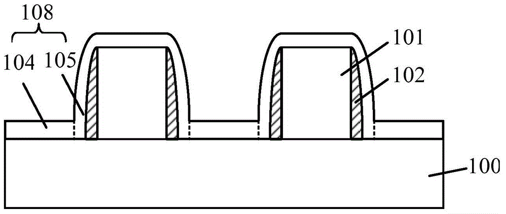
[0035] When the prior art adopts the raised source / drain region formed by the selective epitaxy process, especially when forming the carbon silicon source / drain region, the process is difficult to control, and the formed carbon silicon source / drain region has many defects and relatively high resistance. Big.

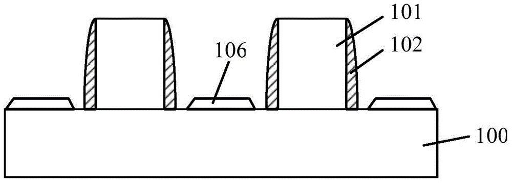
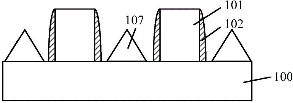
[0036] In order to solve the above problems, an embodiment of the present invention provides a method for forming raised source / drain regions, please refer to Figure 1 ~ Figure 3 , first refer to figure 1 A semiconductor substrate 100 is provided, the material of the semiconductor substrate 100 is a single crystal silicon layer, a gate structure 101 is formed on the semiconductor substrate 100, and sidewalls 102 are formed on both sidewall surfaces of the gate structure 101, so The material of the sidewall 102 is silicon nitride, and grooves (not shown in the figure) may be formed in the semiconductor substrate 100 on both sides of the gate structure 101; figure 1 , ...


PUM


Abstract

According to a semiconductor structure fabrication method, a semiconductor substrate having gate structures is provided. Sidewalls of the gate structures may be covered by a spacer layer. An epitaxy process is performed to form a semiconductor epitaxial material layer covering the gate structures, the spacer layer, and the semiconductor substrate. Then, an etching process is performed to form a first semiconductor epitaxial layer on the semiconductor substrate at the two sides of the gate structures. Further, a selective epitaxy process is performed by using a deposition gas and an etching gas, forming a second semiconductor epitaxial layer. The formed second semiconductor epitaxial layer may repair or compensate the first semiconductor epitaxial layer along the horizontal direction. The epitaxy process, the etching process, and the selective epitaxy process are repeated successively to form elevated source / drain regions. The formed elevated source / drain regions may have a flat top surface without any angles.

Description

technical field [0001] The invention relates to the field of semiconductor manufacturing, in particular to a method for forming a semiconductor structure. Background technique [0002] With the rapid development of semiconductor manufacturing technology, semiconductor devices are developing towards higher component density and higher integration in order to achieve higher computing speed, larger data storage capacity, and more functions. Therefore, Therefore, the gate structure of the complementary metal oxide semiconductor (ComplementaryMetalOxideSemiconductor, CMOS) transistor becomes thinner and shorter than before. In order to obtain better electrical performance, it is usually necessary to improve the performance of semiconductor devices by controlling the carrier mobility. A key element of the technology is controlling the stress in the transistor channel. For example, by properly controlling the stress and increasing the mobility of carriers (electrons in n-channel ...

Claims


Application Information

Patent Timeline
Patent Type & Authority Applications(China)
IPC IPC(8): H01L21/336H01L21/20
CPCH01L29/66H01L21/0237H01L21/02381H01L21/02529H01L21/0262H01L21/02639H01L21/306H01L21/322H01L29/417H01L21/30604H01L21/3065H01L29/41783H01L29/66553H01L29/66628
Inventor 蔡国辉
Owner SEMICON MFG INT (SHANGHAI) CORP
Why Eureka
Try Eureka